


This version (09 Feb 2022 23:01) is a draft.
Approvals: 0/1The Previously approved version (24 Aug 2020 20:30) is available.
Approvals: 0/1The Previously approved version (24 Aug 2020 20:30) is available.
Table of Contents
EVAL-ADXL314-SDP User Guide
FEATURES
- Flexible inertial sensor evaluation platform
- Controller board and interface board operate with interchangeable evaluation boards
- Separates device under test (DUT) from controller for accurate environmental testing
- Data capture at maximum device output data rate (ODR)
- Continuous stream to file data recording
- Standard USB cable for power and communications
- PC-based graphical user interface (GUI)
- Fast, easy installation
GENERAL DESCRIPTION
This user guide describes the evaluation software that interfaces with the ADXL314 accelerometer. For more information on performance details, see the ADXL314 datasheet. The EVAL-SDP-CB1Z is the serial system demonstration platform controller board from Analog Devices, Inc. The SDP-B is part of the Analog Devices system demonstration platform (SDP). SDP controller boards provide a means of communicating with the sensor from the PC. The EVAL-SDP-INTERZ is an SDP interface board. This board serves as an interposer between the SDP controller board and the evaluation board. The interface board is designed to be compatible with various Analog Devices inertial sensor evaluation boards. The EVAL-ADXL314-SDP is an evaluation board that is separate from the interface board to allow easier manipulation of the device for testing (that is, rotating the device around its sensitive axis). The evaluation board is connected to the interface board via a 10-pin cable connector. This user guide provides an overview of how to use the application software. The functionality of the software is described with examples provided where appropriate. Figure 1 shows the required hardware.

Figure 1: what is included in the kit? a) One EVAL-SDP-CB1Z, b) One EVAL-SDP-INTERZ board, c) One EVAL-ADXL314Z board, d) One Standard A to Mini B USB cable, e) Two 10-pin Harwin Datamate L-Tek cable to board connectors, f) One 10-pin Harwin Datamate L-Tek cable connector.
SETTING UP THE EVALUATION SYSTEM
QUICK START
To configure the hardware, follow these steps:
- Install the application software provided (part of the component evaluation package).
- Connect the EVAL-ADXL314Z to the interface board (EVAL-SDP-INTERZ) using the 10-pin cable connector provided.
- Connect the SDP interface board to the SDP-B controller board by clipping the 120-pin connectors together (see Figure 2).
- Connect the Mini B USB cable to the SDP-B controller board and plug the opposite end of the USB cable into the PC. At this point, the set up should look like the one in Figure 3.
- Start the application software.
 Figure 2: Correctly Connected Controller Board and Interface Board: Underside of Controller Board (Left) to Top of Interface Board (Right).
 Figure 3: Fully Assembled Evaluation System.
SOFTWARE STARTUP
When the software first starts, it will ask the user to specify which interface board is being used. There are three revisions of this board (Rev 1 and Rev 2). The user can determine which board you are using by looking at the label in the lower right corner. It will say “SDP Interface Board” (which is Rev 1) or “SDP Interface Board Rev. 2” (which is Rev 2). The user can also look at the 6 digits identifier to determine which revision board you have. 301-522 is the Rev 1 board, 301-621 is the Rev 2 board.
 Figure 4: Software Startup - Hardware Select.
ADXL314 GRAPHICAL USER INTERFACE
 Figure 5: ADXL314 Evaluation Software Startup.
GETTING STARTED
The ADXL314 Customer Evaluation System provide an easy start evaluating the sensor performance. The graphic user interface is divided into separate tabs, each of which specializes in commonly performed measurements for accelerometer devices. In this way, the evaluation system offers users an immediate ability to capture data for a wide variety of tests without the need to develop a customized hardware and software solution.
A brief description of the functionality contained within the evaluation environment is presented in Table 1.
 Table 1: Evaluation Environment Overview.
On each tab, the Start Data Acquisition and Stop Data Acquisition buttons are the primary ways the user acquires data from the device. Click QUIT PROGRAM located in the lower right of the start-up window to exit the software at any time. Other functionalities shared by all tabs are:
Memory Register Map
Provides the ability to read the memory register or to take a snapshot of the current memory register values. Click the Read Register Map button for a snapshot of the current memory register values (see Figure 6). This also updates the serial number and device ID.
 Figure 6: ADXL314 Memory Map and Identification Information.
Software Reset
As described in the ADXL314 data sheet, a software reset command resets the ADXL314 and clears all user applied settings. This returns the part to its default configuration. For example, if the data rate was set to 3200Hz, a software reset will change the data rate to 100Hz (the default). Click the RESTORE DEFAULT CONFIGURATION button (see Figure 7) to perform a software reset of the ADXL314 device. The software reset command can be issued at any time when the software is not busy performing another action. It is important to note that a software reset will also return the part to standby mode. To read acceleration data from the part, it must be placed in measurement mode.
 Figure 7: SOFTWARE RESET Control.
Hardware Reset
To perform a hardware reset of the ADXL314, click the HARDWARE RESET button (see Figure 8). This turns off power to the device. Power off can be observed by monitoring the power LED to the left of the HARDWARE RESET button. If the LED is off, power to the device is off. After power has been off for 5 sec, power is restored. It is important to note that a hardware reset will also return the part to standby mode. To read acceleration data from the part, it must be placed in measurement mode.
 Figure 8: HARDWARE RESET Control.
The following sections describe the purpose of each tab of the software.
DEVICE OVERVIEW TAB
 Figure 9: Device Overview Tab.
The Device Overview tab is a good way to become familiar with how the device operates. This tab contains all the controls to configure the part. For example, when the part first turns on, it powers up in standby mode. The ADXL314 powers up in standby mode to minimize power consumption. To exit standby mode, look at the Power Settings control. Change the mode from standby to measurement mode (see Figure 10).
Figure 9: Device Overview Tab.
The Device Overview tab is a good way to become familiar with how the device operates. This tab contains all the controls to configure the part. For example, when the part first turns on, it powers up in standby mode. The ADXL314 powers up in standby mode to minimize power consumption. To exit standby mode, look at the Power Settings control. Change the mode from standby to measurement mode (see Figure 10).
 Figure 10: Standby to Measurement Mode.
The ADXL314 contains a 3-axis accelerometer, meaning the device is sensitive to acceleration in any direction, whit a fixed range of +/- 200g and a resolution of 13 bits. Please refer to the ADXL314 data sheet for more details.
 Figure 11: Axes of Acceleration Sensitivity (Corresponding Output Increases When Accelerated Along the Sensitive Axis).
The ADXL314 has many user configurable settings to customize its operation for various applications. Configuring the ADXL314 is as simple as selecting the desired option from the drop-down menu. Table 2 shows a summary of the device controls and its respective configuration options list. Default settings are shown in bold.
 Table 2: Device Output Settings (default settings shown in bold).
Select the configuration option to dynamically update the ADXL314 device. For example, changing the sleep data rate from 8 Hz to 1 Hz, as shown in Figure 12 updates the ADXL314 register map immediately. This way, the ADXL314 Memory Map clearly shows how the bits correspond to the applied configuration. For more information on the register map, see the ADXL314 data sheet.
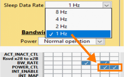 Figure 12: Changing Sleep Data Rate and its effect on the Registers.
Once the part is in Measurement mode, click the Start Data Acquisition button to stream data from the device. The device then continuously streams data until the Stop Data Acquisition button is clicked. The user can experiment by moving the device around to observe the response, which can be plotted on LSB or Gee format (see Figure 13). When the Start Data Acquisition button is pressed while on Device Overview tab, any changes in the Device Output Settings will not take effect and will be overwritten by the values right before the acquisition started. The only exception is the Output Format control.
 Figure 13: Output Format Control configuration options.
There are five interrupts that can be present in the ADXL314 and each corresponds to a different event. These are the DATA_READY, Activity, Inactivity, Watermark, and Overrun interrupts. For a detailed definition of each of these interrupts, see the ADXL314 datasheet.
Figure 14 shows the interrupt controls for INT_ENABLE and INT_MAP as well as the indicators for INT_SOURCE. The INT_ENABLE controls have two states, enabled and disabled. These are all disabled by default. The INT_ENABLE controls determine whether the interrupts can be generated. The INT_MAP controls determine whether the interrupt is mapped to the INT1 or INT2 pin (see device pinout in the ADXL314 datasheet). Each interrupt is mapped to INT1 by default. The INT_SOURCE indicators will each light up when its corresponding interrupt is present.
 Figure 14: Interrupt Settings example. The rounded LEDs show the INT_SORCE register current status.
For example, in Figure 14 the DATA_READY, Watermark, and Overrun interrupts are all present since each of their LEDs is on. However, only the DATA_READY interrupt is mapped to the INT1 pin since it is the only one with its output enabled and mapped to the INT1 pin. The Watermark interrupt is mapped to the INT2 pin. Notice that even though the Overrun interrupt is present (since its LED indicator is on), it is not mapped to any pin because its INT_ENABLE control is disabled. The interrupt controls can be configured in many ways for various applications, including the Auto-Sleep mode.
There are two ways to place the ADXL314 into Auto-Sleep mode. The first is to enable the Auto-Sleep and Link dropdown menus. The Activity and Inactivity interrupts must also be enabled by clicking on them. The second way is to click on the Auto-Sleep Disabled button. The button will highlight and change to Auto-Sleep Enabled. Either method accomplishes the same thing: the part is now in auto-sleep mode. Note that the Activity and Inactivity thresholds, and Inactivity time still need to be set for Auto-Sleep mode to function correctly, as well as the Activity/Inactivity Coupling mode and axis that will trigger the interrupt. The Figure 15 shows an example of the device fully configured on Auto-Sleep mode. The graph shows the device waking up after Activity threshold has been surpassed.
 Figure 15: Example of Device Output Settings configuration for Activity/Inactivity event application.
Note that Activity/Inactivity events require to read the INT_SOURCE register in order to clear the interrupt and get the sensor ready for next Activity/Inactivity event. As explained previously, ones Start Data Acquisition is pressed, registers cannot be read or written. Thus, the acquisition needs to be stopped, which is followed by a registers map update.
DATA RECORD TAB
 Figure 16: Data Record Tab.
The Data Record tab allows the user to measure and record acceleration data. The data is acquired at a user specified data rate and is shown on the plot (see Figure 16). The data is then saved to a text file with the date, time, and device ID recorded as a header. To specify the file path, click the three dots icon under File Path and browse to the desired folder. If an existing file is selected, data is appended to the end of the file. The user can choose a data rate from 6.25 Hz to 3200 Hz with the Data Rate Select control. The remining controls configuration are copied from the Device Overview tab, Device Output Settings.
Figure 17 shows the Match Data Rate control. This tab will acquire data at the rate specified in the Data Rate Select control (100 Hz in this case). When the Match Data Rate control is checked, this tab will match the data rate when the part is in in auto-sleep mode. In other words, when the part is in normal mode, the program will acquire data at 100 Hz. However, when the part is in sleep mode, the program will only acquire data at an 8 Hz data rate to reflect that the part is generating data at a much lower data rate.
Figure 16: Data Record Tab.
The Data Record tab allows the user to measure and record acceleration data. The data is acquired at a user specified data rate and is shown on the plot (see Figure 16). The data is then saved to a text file with the date, time, and device ID recorded as a header. To specify the file path, click the three dots icon under File Path and browse to the desired folder. If an existing file is selected, data is appended to the end of the file. The user can choose a data rate from 6.25 Hz to 3200 Hz with the Data Rate Select control. The remining controls configuration are copied from the Device Overview tab, Device Output Settings.
Figure 17 shows the Match Data Rate control. This tab will acquire data at the rate specified in the Data Rate Select control (100 Hz in this case). When the Match Data Rate control is checked, this tab will match the data rate when the part is in in auto-sleep mode. In other words, when the part is in normal mode, the program will acquire data at 100 Hz. However, when the part is in sleep mode, the program will only acquire data at an 8 Hz data rate to reflect that the part is generating data at a much lower data rate.
 Figure 17: Match Data Rate Control.
Each time the Start Data Acquisition button is clicked, the program starts recording the data to a text file. To select the File Path, click the three dots icon and navigate to the desired folder (see Figure 18). If no directory is specified, the program uses the directory of the current applications as a default. The file name can be specified in the File Name control (see Figure 18). If a file with that name already exists, the data is appended to the end of that file.
 Figure 18: File Path and File Name Controls.
FIFO ANALYSIS TAB
 Figure 19: FIFO Analysis Tab.
The FIFO Analysis tab demonstrates the various FIFO modes available to the ADXL314. FIFO (or First In, First Out) is a method for utilizing a data buffer to prevent loss of data. The user can understand how the different FIFO modes operate by experimenting with the FIFO Demo function. To do this, ensure that the Enable FIFO Demo control is checked. Set the Data Sampling Rate control toward the Slower sampling side of the scroll bar. Make sure it looks similar to Figure 20.
 Figure 20: FIFO Demo Controls.
Ensure that the part is in FIFO mode or Stream mode (not Bypass mode) using the FIFO settings control (Figure 21). Set the FIFO Samples control to 16 (see Figure 22).
 Figure 21: FIFO Mode Control.
 Figure 22: FIFO Samples Control – Updates FIFO Samples Indicator and Memory Register, 0x38 FIFO_CTL.
The FIFO Entries indicator is a direct reading of the FIFO entries bits (Register FIFO_STATUS, Address 0x39, bits [4:0]). This indicator reports how many data values are stored in the FIFO. The FIFO stores a maximum of 31 entries, which equates to a maximum of 32 entries available at a given time because an additional entry is available at the output filter of the device. Click Start Data Acquisition. The FIFO Entries indicator will be full, since the part is generating data much faster than the program is requesting data from the part. It should look similar to Figure 23.
 Figure 23: FIFO Demo - Watermark and Overrun Interrupts.
When the FIFO is full, the watermark and overrun interrupts will be set and their respective LED indicators will be on. The watermark bit is set when the number of samples in the FIFO equals the value stored in the samples bits (Register FIFO_CTL, Address 0x38, bits [4:0]) The overrun bit is set when new data replaces unread data. The overrun bit is automatically cleared when the contents of the FIFO are read. Next, increase the Data Sampling Rate by moving the scroll bar further toward the Faster sampling side as shown in Figure 24.
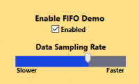 Figure 24: FIFO Demo - Controlling Data Sampling Rate.
The user will see the FIFO Entries value slowly start to decrease. The software is now requesting data slightly faster than the ADXL314 is generating new data. The program is now requesting data faster than the part is generating data. Watch as the FIFO Entries value approaches the FIFO Samples value. As long as the FIFO Entries value is greater than or equal to the FIFO Samples value, the watermark bit will be set. As soon as the FIFO Entries drops below the FIFO samples value, the watermark bit will be cleared (see Figure 25).
 Figure 25: FIFO Demo - Watermark Interrupt.
Now to actually record data from the part using FIFO, disable (uncheck) the Enable FIFO Demo control. This will disable the FIFO demo and will enable FIFO data recording. The software will now request data 5% faster than the set data rate. If the data rate is set to 100 Hz, data will be sampled from the part at a 105 Hz rate. This will ensure that no data is lost. Data can be recorded in FIFO or Stream mode (see Figure 21). FIFO Trigger mode operates differently from the other FIFO modes. This mode collects data centered around an event. This event is triggered by a user defined interrupt.
Complete the following steps to configure the ADXL314 to operate in FIFO Trigger mode as shown in Figure 26:
- Set the Activity Threshold to 4g. Note that it will auto correct to 3.9g since this value increments in 780mg steps.
- Set the Activity/Inactivity Threshold Coupling to AC coupling.
- Enable the x-axis Activity/Inactivity Interrupts.
- Enable the Activity Interrupt from the INT_ENABLE register.
- Set the interrupt to INT2 (INT_MAP register). When the trigger event occurs, it will send the interrupt to the INT2 pin.
- Set FIFO mode to Trigger.
- Set the Trigger source to INT2. When the event occurs, the ADXL314 will look for the trigger in the INT2 pin.
- Set the Samples control to 5. This will save 5 data points before the event occurs.
Now that the ADXL314 is configured, click Start Data Acquisition. Data will be continuously streamed from the ADXL314 until the activity interrupt is triggered. Immediately following this, the ADXL314 will keep the last 5 samples (set in the Samples control) and will then enter FIFO mode. It will then collect another 27 data points immediately following the trigger event. In this way, the ADXL314 will record 5 data points before the event and 27 data points after the event (for a total of 32 data points). Figure 27 shows example data while operating in FIFO Trigger mode. The software streams data from the part until an event is triggered. As soon as the x-axis output increases by more than 3.9g, an activity interrupt is generated and mapped to the INT2 pin. The FIFO settings are set to look at INT2 for the trigger event. As soon as the event occurs the FIFO saves the 5 most recent data points. It then collects another 27 data points to show the output of the part following the trigger event. Data is saved automatically while the test is running. The program creates a header with the date, time stamp, and device ID. The program then records x-, y-, and z-axis acceleration data, INT_SOURCE, FIFO Entries, and FIFO Trigger bit value. Specify the File Path and the file name in the controls at the bottom of the tab. If no directory is entered, the program defaults to the current application directory.
 Figure 26: FIFO Trigger Mode Example.
 Figure 27: FIFO Trigger Mode - Event data.
AUTO-SLEEP TAB
 Figure 28: Auto-Sleep Tab.
The Auto-Sleep tab demonstrates how the auto-sleep mode operates (Figure 28). This feature is very useful for low power consumption applications. The ADXL314 can enter a low power state when it is idle. It can be programmed to wake up when activity is detected (i.e. when the acceleration data changes). The user can configure the part a variety of ways to determine exactly when the part enters sleep mode and when it wakes up. There is a Status indicator in the bottom right corner of this panel (see Figure 28). This indicator will show whether the ADXL314 is operating in normal mode (LED is off) or sleep mode (LED is on). See Figure 29.
 Figure 29: Status Indicator in Sleep (top) and Normal (bottom) mode.
For the ADXL314 to know when to enter sleep mode and when to wake up, activity and inactivity thresholds must be set. These can be set in the Activity Thresholds section (see Figure 30).
 Figure 30: Activity Threshold Controls.
The Activity Threshold determines how much acceleration the part must experience before waking up. If the part is operating in sleep mode, one of the axes must experience 3.9g of acceleration to wake up and enter normal operating mode. The Inactivity Threshold determines when the ADXL314 enters sleep mode. When the part experiences less than 2.34g of acceleration for 5 seconds (the Inactivity Time), the part enters sleep mode. The data output rate and current consumption decrease significantly.
Once the activity/inactivity thresholds are set, the interrupts must still be enabled for each axis. For example, assume that only the x- and y-axes are important for the application. Click the X-Enabled and the Y-Enabled controls to enable these interrupts as shown in Figure 31. To operate correctly, both the Activity Interrupt and Inactivity Interrupt controls must be enabled. On this configuration, only acceleration data in the x- and y-axes is relevant for determining whether the part is in normal or sleep mode. The z-axis is completely irrelevant since its activity and inactivity interrupts are disabled.
 Figure 31: Activity Threshold and Interrupt Enable Controls.
Note that the plot can get a little cluttered when too many axes are plotted. If desired, the user can change the plot visibility by right clicking on a plot in the legend. Click on the Plot Visible option to enable or disable that axis (see Figure 32).
 Figure 32: Control Plot Visibility.
Figure 33 shows the part with Auto-Sleep enabled. In this example, the x-axis and y-axis activity/inactivity interrupts are enabled. This means that only the x- and y-axis outputs will determine whether the part is in normal mode or sleep mode.
 Figure 33: Auto-Sleep Enabled for Two Axes - Sleep Mode Example.
The z-axis is irrelevant in determining the sleep state in this configuration. For this reason, the z-axis is not plotted to improve visibility of the plot (right click on the legend>Plot visible). In this example the part is in Sleep mode. This can be seen by looking at the Status indicator which will say “Sleep mode” or “Normal Mode”. In addition, the background of the plot will darken to indicate that the part is in sleep mode. The Activity and Inactivity thresholds are set to 2.34g. DC threshold coupling is used so the detection levels are at ±2.34g. This means that if either the x-axis or y-axis acceleration exceeds 2.34g magnitude, the part will wake up and exit sleep mode. This is shown in Figure 34. The y-axis acceleration exceeds 2.34g and the activity interrupt is generated, waking the part up. Note that the Status indicator now shows “Normal Mode” and the plot background is white. In order to enter sleep mode again, both the x- and y-axis outputs must have magnitudes less than 2.34g. Note that the black horizontal lines indicate DC thresholds. Blue, red, or green horizontal lines indicate AC thresholds.
 Figure 34: Auto-Sleep Enabled for Two Axes - Wake up Example.
Figure 35 shows the part with Auto-Sleep enabled. In this example, only the x-axis activity/inactivity interrupts are enabled. This means that only the x-axis output will determine whether the part is in normal mode or sleep mode. The y- and z-axis outputs are irrelevant in determining the sleep state in this configuration. For this reason, the y- and z-axis are not plotted to improve visibility of the plot (right click on the legend>Plot visible).
 Figure 35: Auto-Sleep Enabled for Single Axis - Sleep Mode Example.
In this example the part is already in sleep mode. This can be seen by looking at the Status indicator which will say “Sleep mode” or “Normal Mode”. In addition, the background of the plot will darken to indicate that the part is in sleep mode. The Activity and Inactivity thresholds are set to 2.34g. AC threshold coupling is used so the detection levels are at ±2.34g. Unlike DC coupling, these thresholds are not centered around 0g. Instead they are centered around the output acceleration when the auto-sleep mode was activated. In this example the thresholds are set at 3.24g and -1.64g. Therefore, when the auto-sleep was activated, the x-axis output was 0.9g. If the x-axis remains within ±2.34g of 0.9g, the part will remain in sleep mode. As soon as the x-axis exceeds either of the thresholds, the part will wake up and enter normal mode, as shown in the Figure 36.
 Figure 36: Auto-Sleep Enabled for Single Axis - Sleep Mode Example.
The thresholds will update any time the acceleration exceeds the AC thresholds. Note that the activity and inactivity thresholds need not be set to the same value. This was done here for simplicity. However, the inactivity threshold should always be less than or equal to the activity threshold for the auto-sleep to function properly.
TILT MEASUREMENT TAB
The ADXL314 is a 3-axis accelerometer, and as such can provide inclination sensing. Data is acquired at the user specified data rate. The x-, y-, and z-axis acceleration data is plotted in real time on the main chart. The software acquires data for 250ms, averages the results, and plots the average value on the main chart. In other words, each data point is an average of 250ms of data from the part. In addition, the two images in the lower right corner show the front view and the side view of an example vehicle. This give a more visual representation of the inclination data (see Figure 37).
 Figure 37: Tilt Measurement Tab.
In order to obtain accurate results, the software allows calibration of the ADXL314. Click the Calibrate XL button to begin. Following this, a series of 6 pop-up dialog boxes will appear. Follow the instructions in these dialog boxes. They will instruct you to hold the evaluation board in specific orientations such that each axis is exposed to a ±1g field (see Figure 38).
 Figure 38: Calibration Orientation. X-axis 1g field (left), Z-axis 1g field (right).
The offset and sensitivity calibration coefficient are then calculated for each axis (see Figure 39). The following example provides clarity on the process.
- Place the x-axis in a +1g field. Hold the evaluation board vertically on a flat surface as shown on the left side of Figure 38.
- Click OK and hold the part still for 1 second.
- Reorient the part as shown in the next dialog box.
- Repeat until all 6 measurements have been completed.
 Figure 39: Calibration Results.
Using the y-axis as an example, the measured outputs when the y-axis was placed in a ±1g field were as follows:
Therefore, the offset can be calculated according to the following formula:
And the sensitivity can be calculated according to the following formula:
This demonstrates how the values in Figure 39 were calculated.
SELF-TEST TAB
 Figure 40: On-Demand Self-Test Tab.
The ADXL314 incorporates a self-test feature that effectively tests its mechanical and electronic systems simultaneously. When the self-test function is enabled, an electrostatic force is exerted on the mechanical sensor. This electrostatic force moves the mechanical sensing element in the same manner as acceleration, and it is additive to the acceleration experienced by the device. This added electrostatic force results in an output change in the x-, y-, and z-axes. The Self-Test tab demonstrates how this function operates for each axis (see Figure 40). Once the Start Data Acquisition button is clicked, the software acquires one second of data from the ADXL314 at the user specified data rate.
- For the first 250ms, the self-test feature is disabled (default state).
- At 250ms the self-test bit is asserted, and the self-test function begins. An electrostatic force is applied to the beam. This causes the output to shift as shown in Figure 40.
- The self-test bit is asserted for 500ms.
- At 750ms the self-test bit is de-asserted and the device output return to normal.
Acceptable values for self-test output are shown in Table 3.
 Table 3: Self-Test Output in g’s (TA = 25°C, 2.0 ≤ VS ≤ 3.6).
POWER CYCLE TAB
 Figure 41: Power Cycle Tab.
Use the Power Cycle tab to determine the turn-on to turn-on variability of the ADXL314. The device undergoes a hardware reset followed by a series of internal diagnostic routines to ensure the integrity of its various signal chains. Following these procedures, acquisition of acceleration information from the MEMS sensors begins. This will continue until the software has completed the number of cycles specified by the user. Or if the Run Continuously box was checked, the software will run until the Stop Data Acquisition button is clicked. Using the Power Cycle Controls, specify the off time, the on time, and the number of power cycles. The off time sets the length of time that power to the device is turned off. Following this, power is restored and data is acquired for the specified length of time. The average value is then plotted on the graph. The output from each inertial channel is plotted after each power cycle.
Figure 41 shows example settings for these controls. In this example, the software is set to run 50 power cycles. Each cycle begins by turning power off for 250ms then turning power on and acquiring data for 500ms. This 500ms of data is then averaged together and plotted on the main chart as a single point. If the Run Continuously box is unchecked, the software will cycle the power 50 times and then stop, which is the case of the example of Figure 41. If the Run Continuously box is checked, the Set Number of Power Cycles control will be disabled and greyed out. The software will then continue cycling the power and acquiring data until the Stop Data Acquisition button is clicked.
After each cycle, the current data is updated in the Current Data table to the left of the Power Cycle Controls. This table includes information from the most recent cycle for each inertial channel.
TURN-ON ANALYSIS TAB
 Figure 42: Turn-On Analysis Tab.
In addition to the bias stability from one power cycle to the next, it is important to understand the device behavior at the moment power is applied to the device. The Turn-on Analysis tab demonstrates the transient response when the device first powers up.
By pressing Start Acquisition data, a hardware reset turns power to the device off for 5 sec. Power is then restored and data is acquired at the user specified data rate.
Figure 42 shows an example of the turn-on characteristics of the ADXL314 after a software reset. 500ms of data is acquired to demonstrate the turn-on behavior of the ADXL314.
MOSI COMMAND GENERATOR TAB
 Figure 43: MOSI Command Generator Tab.
The MOSI Command Generator tab is a useful tool for quickly generating any read or write command for the ADXL314 with the correct CRC. Click a choice from the Select Memory Register drop down menu to select the desired register to read or write to (see Figure 44).
 Figure 44: Select Memory Register Control.
Select READ or WRITE from the Command Type drop down menu (see Figure 45).
 Figure 45: Command Type Control.
Figure 46 shows an example of a MOSI write command to write a value of 0x1F to the x-axis offset register (OFSX, Register 0x1E). For this device, the value of 0x1F written to OFSX register, adds a +6g offset to the x-axis. Thus, in a 0g field the x-axis will still output 6g. Click the Calculate MOSI Command button to update the Full MOSI Command output shown on the right side of Figure 46 (0x00001E1F).
 Figure 46: Write Command to Control Register 0x1E (OFSX).
Press Start Acquisition data button if you wish to visualize the MOSI command created on the ADXL314 Register Map. The OFSX register will now display the offset added to the x-axis output as shown in the Figure 47.
 Figure 47: Write Value of 0x1F to OFSX Register.
Figure 48 explains what each field of the MOSI command represents for a write command. A ‘0’ in the most significant digit (shown in green) indicates that this is a MOSI write command. The address field (shown in orange) is 6 bits long and indicates to which address the write command is addressed. The last 8 bits (shown in blue) contain the write data to be written to the register specified in the address field. The example in Figure 48 shows a write command to register 0x27 (ACT_INACT_CTL).
 Figure 48: Explanation of MOSI Write Command Fields.
Figure 49 explains what each field of the MOSI command represents for a read command. A ‘1’ in the most significant digit indicates that this is a MOSI read command. The next digit is the multi-byte read. If this digit is ‘0’, the command will read a single register specified by the address field. In the example in Figure 49, a multi-byte read starting with address 0x32 (DATA_X0). If 5 more bytes of 0’s are sent after this, the MISO response will contain read data of all the inertial data channels (DATA_X0 to DATA_Z1). In this way, acceleration data from x-, y-, and z-axis channels can be read with a single command.
 Figure 49: Explanation of MOSI Read Command and MISO Response.
resources/eval/user-guides/inertial-mems/accelerometers/adxl314/eval-adxl314-sdp.txt · Last modified: 09 Feb 2022 23:01 by Pablo del Corro