


This version (01 Mar 2018 03:41) was approved by Jeff Watson.The Previously approved version (23 Feb 2018 23:37) is available.
Table of Contents
EV-HT-200CDAQ1 Firmware Guide
Purpose
This document is intended to provide firmware developers an introduction into the code structure and specifics on some of the time critical functions. It should be used in conjunction with the EV-HT-200CDAQ1 / HT-DAB-1 Keil MDK project that is available on the ADI GitHub
The project controls the activity of the EV-HT-200CDAQ1, which has three Analog Devices ADCs, an analog multiplexer and conditioning circuitry. Users can send commands to the board via a PC (COM port over USB). The board will respond by either executing the command or issuing an error message. Responses to commands are transmitted on the UART back to the PC.
Source and Header File Organization
The project is organized into .c and .h files. The following tables summarizes the contents of more salient files.

Firmware Function Overview
A simplified flow diagram is shown in below. The ADC sampling engine is time critical and is explained in a later section.
 EV-HT-200CDAQ1 Firmware Flowchart
 Parser Routine Flow
Mode and Status Parameters
As commands are entered and data is collected, there are important state parameters used to coordinate the sampling engine and the UART output activity. The table below lists the most important enumerations for the project.

MCU Resource Use
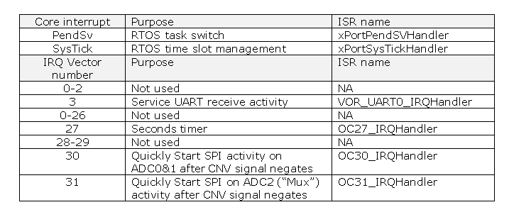
This section has tables showing the pins, peripherals and interrupts used in the project. All other GPIO pins, timers and peripherals can be used by the end user’s application.

MCU Pin Use Table

Peripheral and Timer Use Table

Interrupt Vector Use Table
UART input ("uart.c")
A PC will be able to send information to the MCU via a USB to UART converter. The PC can command various activities including: a conversion sequence to begin, set a second counter value or request a temperature reading.
UART settings are:
- Baud rate = 2 Mbits/sec, 8-bits data, 0 parity, 1 stop (8N1)
- Hardware handshaking enabled. (CTS/RTS) {Note: RTS is not physically connected. Data coming from PC to MCU will be minimal and the MC’s UART will not overflow.}
- No CRC on frame
UART receive software is implemented in an ISR when the FIFO buffer has information available. Inside the ISR, a character string is buffered in a 128-byte array, with start pointer = *pui8RxHead.
Parsing (“parser.c”)
As part of the main loop, the “ParseCommand” function is called. This will analyze the UART “RxBuffer”. When an end of string character (“\r”) is received, the string is compared against valid commands. All command strings begin with “$”. Invalid command strings will result in an “$ERROR:” response on the UART transmitter. Using the backspace character to correct typing errors is allowed. The use of the back and forward arrows to edit an input string is not supported.
Valid commands will prompt further actions. Status and Mode information is set for a subset of the commands in global variables “m_iStatus” with “StatusEnum” enumeration and “m_iRunMode” with “runModeEnum” enumeration. This information is used inside the UART output and ADC convert engines.
ADC sampling (“sampling_engine.c”)
When prompted via a valid UART command, an ADC sampling sequence (“experiment”) is initiated. “m_iStatus” and “m_iRunMode” variables indicate a pending experiment. There are four cases possible:
- Iterative Burst mode (Iteration rate set by “$setexp” command)
- Single shot burst mode
- Continuous mode
- External trigger burst mode.
For iterative burst and single shot burst, the second (1/60 of a minute) counter ISR will check the status and mode information and commence the experiment. That will force the first experiment in these two modes to align with the second counter rollover event.
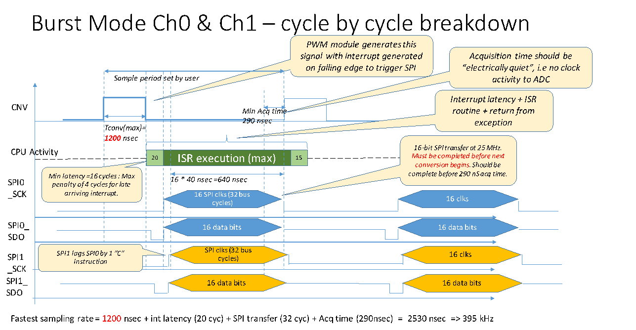
The MCU will use the SPI interface to clock data out of the ADC. The conversion start signal is generated with a timer which allows precise sampling period control and a precise pulse width needed for the CNV input signal to the ADC. Before the next conversion starts, the data from the present conversion is clocked out completely. This will eliminate any clock noise from corrupting the analog input during the conversion time.
The ADC Data Out signal will go to a high impedance state when a conversion is being made. To reduce current consumption and eliminate potential switching noise, the MCU’s internal pull-up resistor (~33kΩ) is enabled on all MISO pins.
The ADC servicing is done in the timer interrupt service routine. The conversion will begin on the rising edge of a timer output and the ISR is called on the falling edge as shown in diagram below.

Data collected from the ADC is stored in a dedicated 16kbyte (16,384) buffer that will later be sent out a UART port to a PC host. The buffer can be divided into segments for different ADC channels as set by the incoming command. The 16kbyte buffer is storing 16-bit conversions, thus this is an 8Ksample buffer.
To achieve the fastest sampling rate, software was written in a non-conventional way and the compiler optimization must be set to level 3 for maximum performance. Some compilers automatically store all registers before starting an ISR. This is not allowed if 2.4ųs conversion rates are expected.
SPI Setup
The SPI clock is set to 25 MHz. This is half the MCU system clock and the fastest achievable SPI master clock from the VA10800. Special settings are required to make this operate correctly at this speed. The data in (MISO) of the MCU must be setup to capture the ADC’s output on the falling edge of the SPI SCK signal. The filtering for these pins must be disabled and the synchronous setting disabled. FILTER = 0x1.

Aligning CNV signals for ADC0 & ADC1
One of the sampling timing requirements is that the CNV signals for ADC0 and ADC1 being exactly aligned. This is accomplished by using the cascade function of the Vorago timers. One timer, TIM_0, is used to trigger two other timers that create the CNV signals using the PWM function.

External Trigger Mode
External trigger mode allows an external signal to dictate when a burst experiment commences. To still allow simultaneous conversions on ADC0 and ADC1, the same scheme as outlined in section 6.2 is used with the addition of TIM0 being triggered using its cascade 1 input from PORTB[14] pin interrupt. As a rising edge is detected on PORTB[14], an interrupt request is generated which will put TIM0 in active mode which will quickly count to zero and trigger TIM2 and TIM20. Note that the pin interrupt does not generate an interrupt to the CPU since the IRQSEL peripheral is not configured to do this.
VCC and RTD Sampling with Burst
The viewer program on the PC expects VCC and RTD information to go along with every burst sequence. Four samples of channel 8 (VCC) and channel 9 (RTD) are conducted at the end of each burst sequence. An average is calculated and reported as the first line of each Burst experiment UART output sequence. The sample rate for these conversions is set to 10ųs independent of what the $setacq calls out. This was done to ensure the analog multiplexer and associated op-amp have time to stabilize.
UART output (“output.c” & “uart.c”)
The UART is the primary communication channel from the MCU to a user. It is routed through a UART to USB converter to a PC’s USB port. A virtual serial communication port program such as PuTTY can be used to collect the data. (TeraTerm did not support 2Mbit/sec rates and could not be used)
UART settings are:
- Baud rate = 2 Mbits/sec, 8 bits data, 0 parity, 1 stop (8N1)
- Flow control signals must be used. Windows OS only services the COM ports periodically and if there are several programs running or the display is being refreshed, the PC cannot keep up with 2Mbit/sec data flow. It was required to implement CTS on the MCU to gate the transmission of data.
- No CRC on frame. (No acknowledgement on message being received)
Data buffered from the ADC is stored in 16-bit integer format. Data sent out the UART will be a 5-byte stream in hexadecimal ASCII including a “comma” delimiter. (i.e. ABCD,1234,)
Free RTOS Shell
The code is written in a FreeRTOS shell. This will allow users to create their own code without interfering with the data acquisition and reporting processes. A compiler directive in “ht_dab_user.h” can enable or disable the use of FreeRTOS. By commenting out the line with “#define USE_RTOS 1”, the RTOS code is removed from the project.
The downloaded version of FreeRTOS will completely stop all interrupts from occurring for a short period during the task change. For sampling rates of 4us or less, this can result in corrupt ADC reads. Software has been added to check for the sampling rate and to temporarily disable the RTOS during an experiment.
The below diagram shows the priority hierarchy. The OS will jump between the data acquisition task and the User task. Interrupts are implemented for the ADC sampling, the tick timer and the UART receive process. Either the data acquisition task or the user task can be interrupted when one of these events occurs.

Due to some inherent interrupt blocking of FreeRTOS during task changes, a conflict can arise when the ADCs are being converted very rapidly, under 4us. During an acquisition experiment with sampling rate under 4us, the RTOS is temporarily disabled.
Housekeeping
Watchdog Timer
One timer is used to create a watchdog timer. If the timer is not serviced within a countdown interval, the MCU will be RESET and the RESET source will be WATCHDOG. The watchdog period is defined in ht_dab_user.h.
Unused Port Pins
All unused port pins are terminated using an internal pull-down resistor. This reduces current draw from floating inputs.
Temperature and Vcc Calculation
The RTD data sheet contains a table with resistance values for every 1°C. Firmware has created a linear interpolation conversion program for 5 different regions in the -55°C to 200°C range.
Both the RTD and VCC calculations account for a voltage divider network.
RTD and VCC calculations were modified to account for two 100kΩ resistors used to bias the output of the Analog Multiplexor. See the schematic for details on this.
Performance
This section contains information on the MCU response time, maximum conversion rates and approximate code size for various tasks.
ADC Sample Rate
As shown in the below diagram, the fastest ADC sample rate using interrupt is 413 kHz which corresponds to 2.4ųs.

UART RX Performance
The MCU must be able to receive a 64-character string from the host PC at a baud rate of 2Mbps. This type of packet will not happen in rapid succession.
UART TX Performance
Due to bandwidth limitations of a PC’s USB port, flow control (CTS signal enabled) must be implemented on the UART transmitter. The UART module will automatically pause when the PC is not ready to accept more characters. The Tx performance is 100% dependent on the PC capability. We have seen cases where display refresh activity can slow the USB port down immensely.
If transmission of sample data does not complete before the next sampling period, the next sampling period will be dropped entirely with no message.
CPU Processing Margin and Memory Use
The RTOS scheduler is allocating 50% of the CPU bandwidth for handling the acquisition task. Some activities are interrupt driven and the actual CPU cycles spent on these are dependent on sampling rate and amount of data being transmitted to a PC. The following table can be used to estimate the available CPU bandwidth.

Compiler and IDE
The initial firmware package was developed and tested using the Keil µvision IDE revision 5.23. The code size is below 32k and the free evaluation version can be used.
resources/eval/user-guides/high-temp/ev-ht-200cdaq1/firmware.txt · Last modified: 01 Mar 2018 03:41 by Jeff Watson