


This version is outdated by a newer approved version. This version (18 Mar 2022 18:12) was approved by Antonio Jimenez de Parga.
This version (18 Mar 2022 18:12) was approved by Antonio Jimenez de Parga.This is an old revision of the document!
Table of Contents
EVAL-AD3542R Evaluation Board User Guide
Evaluation Board for the AD3542R, Dual Channel, 16-Bit, 16 MUPS, Multispan, Multi-IO SPI DAC
Features
- Full featured evaluation board for the AD3542R
- Selectable transimpedance gain
- Selectable transimpedance amplifier supplies
- On-board or external power supply
- On-board or external voltage reference
- Several impedance matching options
- Clock and trigger inputs for external synchronization
- Mates with controller board SDP-H1
Evaluation Kit Contents
- EVAL-AD3542RFMCZ
Hardware Required
- SDP-H1 board, must be purchased separately
Software Required
- ACE Software
- AD35X2R ACE Plugin (automatically downloaded within ACE)
General Description
The EVAL-AD3542RFMCZ is an evaluation board for the AD3542R ultrafast 16-bit precision DAC.
The board allows testing all the output ranges of the DAC, waveform generation, power supply and reference options.
The EVAL-AD3542RFMCZ interfaces to the USB port of a PC via a system demonstration platform (SDP-H1 board). It can also be connected to a different controller board using the pin header connector at position P5.
This user guide covers the details of the configuration and operation of the EVAL-AD3542RFMCZ board and the associated ACE plug-in. For additional information on the DAC operation refer to the AD3542R data sheet.
Evaluation Board Photograph


Evaluation Board Quick Start Procedure
Installing The Software
The EVAL-AD3542R uses the ACE software with the AD35X2R Plugin for evaluation.
- Click on the Plugin Manager item on the left-hand menu as shown in Figure 1.
- Go to Available Packages, select Board.AD35X2R and click on the Install Selected button at the bottom of the list. Once the plugin is installed, it moves to the Installed Packages section.
- Click on the Home item on the left-hand menu. If the EVAL-AD3542R board is connected it will show up in the Attached Hardware section as shown in Figure 2. If you don't have an EVAL-AD3542R board, you can still explore the functionality of the plugin by double clicking on the desired board in the Explore Without Hardware list.
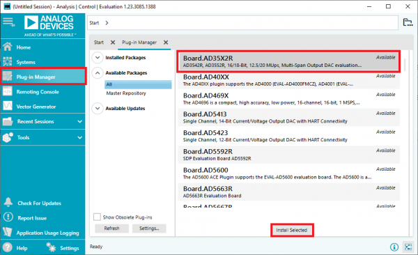
Figure 1. Plug-in Manager

Figure 2. Start Tab
Connecting The Board
To set up the evaluation board, take the following steps:
- Make sure that all the links are set in the default positions listed in Table 2.
- Plug the EVAL-AD3542R evaluation board on the SDP-H1 controller board.
- Connect the wall-plug brick power supply to the SDP-H1 DC jack and power from the AC network. Power LEDs on the SDP-H1 board turn on green.
- Connect the USB cable between the SDP-H1 board and the PC.
- ACE should now be able to detect the board and show it in the Attached Hardware section, as shown in Figure 2. Double click on the board icon to open the board view, as seen in Figure 5. The board view shows the relevant parts included in the evaluation board, where the AD3542R chip is highlighted in a darker blue.
Evaluation Board Hardware
Power Supplies
The EVAL-AD3542R includes a complete power conversion solution to allow powering the evaluation board from the SDP-H1. The board includes a DC/DC converter LTC7149 to generate -7V from the 12V power provided by SDP-H1. LDOs LT3045 and LT3094 are used to generate the positive and negative supplies for the transimpedance amplifiers, which are selectable using switch S1. Additional LT3045 LDOs are used to generate the supplies for the logic and the DAC core of the AD3542R. This power solution is configured with the default link settings shown in Table 2.
Alternatively, the board can be powered from a collection of external power supplies via connector P3. The assignment of the pins in connector P3 is listed in Table 1.
Table 1. Pin Assignment on Power Supply Connector P3
| Pin Number | Signal | Description |
|---|---|---|
| 1 | EXT_PVDD | External positive supply for transconductance amplifiers. 4.7V to 10.6V ± 5%. |
| 2 | EXT_PVSS | External negative supply for transconductance amplifiers. 0V down to PVDD-10.6V ± 5%. |
| 3 | EXT_VDD | External analog supply for AD3542R. 5V ± 5%. |
| 4 | EXT_DVDD | External digital supply for AD3542R. 1.8V ± 5%. |
| 5 | EXT_VLOGIC | External digital I/O supply for AD3542R. 1.1V to 1.9V. |
| 6 | GND | Ground. |
The EVAL- AD3542R also integrates an on-board 2.5V analog reference ADR4525.
Power Supply Configuration for Transimpedance Amplifier
The supply for the transimpedance amplifier integrated in AD3542R must be adjusted depending on the selected output span using switch S1. Table 2 presents the three possible supply configurations. The correspondence with the output range is shown in Table 7.
Table 2. Transimpedance Amplifier Supply Options
| S1 Position | Label | PVDD Voltage | PVSS Voltage |
|---|---|---|---|
| Left | +/- 5V | 5.2V | -5.2V |
| Middle | 10V | 10.2V | -0.2V |
| Right | -2.5/7V | 7.7V | -2.7V |
Do not change the position of S1 while the board is powered up.
Link Options
The EVAL-AD3542R board is delivered with the links placed in the default positions listed in Table 3. This configuration is suitable for operating the board right out of the box. However, the links J_FB0, J_FB1 and J_REF may need to be adjusted depending on the configuration set in the registers of the AD3542R. Refer to Figure 3 to locate the position of links and connectors.

Figure 3. Board Layout
Table 3. Link Options
| Link | Silkscreen | Description | Default Position |
|---|---|---|---|
| J_FB0 | FB0 | This link selects the gain of transimpedance amplifier for channel 0. The gains are labeled x1 and x2 which corresponds to the multiplicative factor between them. The gain must be set in accordance to the desired output range listed in Table 6. Inserting the link allows selecting gains x1 or x2. | x1 |
| J_FB1 | FB1 | This link selects the gain of transimpedance amplifier for channel 0. The gains are labeled x1 and x2 which corresponds to the multiplicative factor between them. The gain must be set in accordance to the desired output range listed in Table 6. Inserting the link allows selecting gains x1 or x2. | x1 |
| J_OUT0 | J_OUT0 | This link bridges the output voltage of DAC0 to connector VOUT0 through the matching network R4, L5, R28, C15. When inserted, signal can be measured on connector VOUT0. When not inserted, signal can only be measured on test point TP2. | Inserted |
| J_OUT1 | J_OUT1 | This link bridges the output voltage of DAC1 to connector VOUT1 through the matching network R5, L6, R29, C16. When inserted, signal can be measured on connector VOUT1. When not inserted, signal can only be measured on test point TP3. | Inserted |
| J_REF | J_REF | This link allows connecting the on-board reference to AD3542R. This link should be removed if an external reference is provided via connector J1 (VREF) or if the internal reference is output to the VREF pin. | Inserted |
| J_PVDD | PVDD | This link selects the positive voltage supply for the transimpedance amplifier. REG selects the supply from the on-board LDO. EXT selects the supply provided externally on connector P3. | REG |
| J_PVSS | PVSS | This link selects the negative voltage supply for the transimpedance amplifier. REG selects the supply from the on-board LDO. EXT selects the supply provided externally on connector P3. GND sets the supply rail to ground. | REG |
| J_VDD | VDD | This link selects the voltage supply for the analog section of AD3542R. REG selects the 5V supply from the on-board LDO regulator. EXT selects the supply provided externally on connector P3. | REG |
| J_DVDD | DVDD | This link selects the voltage supply for the digital section of AD3542R. 1V8 REG selects the supply from the on-board LDO regulator. FPGA selects the supply provided from the SDP-H1 board, the same as used in the FPGA IO pins. EXT selects the supply provided externally on connector P3. | 1V8 REG |
| J_VIO | VLOGIC | This link selects the voltage supply for AD3542R IO pins. 1V8 REG selects the supply for the on-board LDO regulator. FPGA selects the supply provided from the SDP-H1 board, the same as used in the FPGA IO pins. EXT selects the supply provided externally on connector P3. | 1V8 REG |
| S1 | S1 | This switch selects one of the following combinations for PVDD and PVSS: • Left: PVDD = 5.2V, PVSS=-5.2V • Middle: PVDD = 10.2V, PVSS = -0.2V • Right: PVDD = 7.7V, PVSS = -2.7V | Left +/- 5V |
On-Board Connectors
Table 4 shows the list of connectors available on EVAL-AD3542R and their corresponding use. Refer to Figure 3 to find their location in the board.
Table 4. List of Connectors
| Connector | Silkscreen | Signal Name | Function |
|---|---|---|---|
| J1 | VREF | VREF | Reference voltage input / output. This connector can be used to provide an external reference voltage to the AD3542R or to monitor the reference generated by ADR4525 or AD3542R. |
| J2 | CLOCK | CLOCK_FMC | External clock reference provided to the FPGA to generate the SPI patterns. 1.8V amplitude. |
| J3 | SYNC | SYNC_EVENTS | External trigger signal provided to the FPGA to synchronize waveform generation. 1.8V amplitude. |
| VOUT0 | VOUT0 | VOUT0_C | Voltage output of DAC channel 0. |
| VOUT1 | VOUT1 | VOUT1_C | Voltage output of DAC channel 1. |
| P1 | P1 | - | FMC connector carrying the digital signals between the evaluation board and the controller board. |
| P3 | P3 | - | External supply connector. Pin assignment given in Table 1. |
| P5 | P5 | - | Digital signal connector. This connector is used to control the AD3542R with a controller different from SDP-H1. The pin assignment is listed in Table 4. The pin header is not assembled by default so that the holes can be used as test points for the digital signals. |
Connector P5 is used to connect an external controller when the SDP-H1 is not present. This connector grants access to all the digital signals of AD3542R and some board supplies and control lines.
Table 5. Pin Assignment on Connector P5
| Pin number | Connector Label | Function |
|---|---|---|
| 1 | +12V_FMC | External 12V power supply. Use this pin to supply the EVAL-AD3542R board when using a controller different from the SDP-H1. |
| 2 | POWER_ON_FMC | Enable signal for the onboard regulators. This pin is used to manually turn on the LDOs and DC/DC converter when the SDP-H1 controller is not present. Set a voltage higher than 1.24V to turn on. |
| 3 | GND | Ground. |
| 4 | SPI_QPI | Connected to FPGA. Not used. |
| 5 | VLOGIC | Voltage supply used for AD3542R I/O pins. If this pin is used to supply VLOGIC, remove the link for VLOGIC. |
| 6 | GND | Ground. |
| 7 | SPI_CS | SPI Chip Select signal. |
| 8 | SPI_SCLK | SPI clock signal. |
| 9 | GND | Ground. |
| 10 | SPI_SDIO0 | SDI / MOSI signal in Classic SPI mode or SDIO0 signal in Dual SPI mode. |
| 11 | GND | Ground. |
| 12 | SPI_SDIO1 | SDO / MISO signal in Classic SPI mode or SDIO1 signal in Dual SPI mode. |
| 13 | CLOCK_FMC | External clock signal (same as connector J2). |
| 14 | GND | Ground. |
| 15 | LDAC | AD3542R LDAC signal. |
| 16 | GND | Ground. |
| 17 | RESET | AD3542R RESET signal. |
| 18 | GND | Ground. |
| 19 | ALERT | AD3542R ALERT signal. |
| 20 | VLOGIC_FMC | Test Pin for VLOGIC_FMC power supplied from the SDP-H1. |
The board includes several test points to access relevant signals. Only TP4 has the test ring assembled. The list is given in Table 6.
Table 6. List of Test Points
| Test Point | Signal | Description |
|---|---|---|
| TP1 | VREF | Reference voltage for AD3542R (internal, on-board or external) |
| TP2 | VOUT0 | Voltage output of DAC channel 0 |
| TP3 | VOUT1 | Voltage output of DAC channel 1 |
| TP4 | GND | Ground |
| TP7 | GPIO_9 | Synchronization signal from FPGA for development purposes |
| TP8 | SYNC_EVENT | External trigger for waveform generation |
DAC Output Range Selection
The selection of the output range requires a combination of register configurations and a given transimpedance gain. The supply of the transimpedance amplifier must be adjusted accordingly. The gains corresponding to each output range and the required board configuration are listed in Table 7. See the AD3542R datasheet for more details on output range configuration.
Table 7. Transimpedance Gain Setting
| CHx_OUTPUT_RANGE_SEL Field Value | Output Range | Transimpedance Gain Setting | S1 Setting | VZS (V) | VFS (V) |
|---|---|---|---|---|---|
| 000 | 2.5V | x1 | Any | -0.198 | 2.697 |
| 001 | 5V | x1 | Any | -0.077 | 5.076 |
| 010 | 10V | x2 | Middle | -0.163 | 10.163 |
| 011 | ±5V | x2 | Left | -5.163 | 5.166 |
| 100 | -2.5V to 7.5V | x2 | Right | -2.666 | 7.662 |
DAC Output Monitoring
Monitoring the output of the DAC in dynamic conditions can become difficult because the amplifier is a low-impedance source driving a high-impedance load with a fast rising time. The EVAL-AD3542R allows using different passive networks to adapt the output of the DAC to different loads. The following configurations are foreseen:
- Using a high-impedance probe on test points TP2 and TP3. Oscilloscope probes, active or passive, have high impedance. However, since the test points are close to the driver the effect of impedance mismatch is not visible. The main drawback is the tolerance of the probe ratio and the noise picked up in the ground lead. This method is suitable for quick checks and slew rate measurement.
- Using a coaxial cable with the oscilloscope in high impedance. This solution reduces noise pick-up and eliminates the uncertainty of the probe, allowing accurate measurements with dynamic signals, such as settling time. To attenuate reflections from the oscilloscope, 47Ω resistors are included by default in positions R4 and R5. This configuration can be used to measure the output noise density with the oscilloscope configured in AC mode.
- Using a coaxial cable with the oscilloscope in 50Ω impedance. A matching pad must be used so that the impedance seen at the coaxial connector is 50Ω. For example, 976Ω for R4 or R5, 52.3Ω for R28 or R29 and 0Ω for C15 or C16. This solution provides perfect impedance matching on both sides of the coaxial cable while the DAC sees 1kΩ load. The signal is attenuated by a factor 19.55 (25.8 dB). This configuration can be used to measure settling time very accurately. It is not suitable for noise measurements because the attenuation of the matching pad sets the noise below the sensitivity of the spectrum analyzer.
- Using a coaxial cable to drive a medium-impedance load, for example 500Ω. This configuration is half-way between perfect impedance matching and high-impedance termination. It provides better matching in high speed, lower noise susceptibility and lower power dissipation with DC voltage. The driver is series-terminated to 47Ω (R4 or R5) to match the nominal impedance of the cable while the receiver is terminated to 500Ω (for example, an oscilloscope in 1MΩ impedance with 500Ω on a Tee connector). To minimize DC loss, 1μH inductors are used at L5 and L6. A snubber network can be added on R28, R29, C15 and C16 to reduce the overshoot caused by these inductors.
ACE Plug-In Description And Features
ACE Plug-In Hierarchy
ACE has several views to control different aspects of the DAC. When a view is first opened it creates a new tab at the top of the main window. The AD3542R plugin has a Board View, a Chip View, a Memory Map view, a Waveform Generator view, and a Vector Generator view. Figure 4 shows the hierarchical relation between these views. For additional information refer to the The user manual that is accessible from the help panel displayed when clicking on the Help button on the lower left angle of the application. There is also an ACE Wiki with additional information.

Figure 4. ACE Plugin Hierarchy

Board View
The board view displays a simplified diagram of the evaluation board including some relevant connectors and the interconnection between chips, as seen in Figure 5. Analog Devices chips are shown with their part number and the AD3542R is highlighted in darker blue.

Figure 5. AD3542R Board View
The actions that can be performed at this level are displayed as buttons at the top of the main window, as seen in Figure 6.
- Poll Device: this action is performed automatically every second to verify that the evaluation board is connected to the system. The button allows turning on or off this feature.
- Reset Board: this action performs a power cycle on the evaluation board, bringing everything back to default.
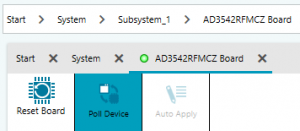
Figure 6. AD3542R Board View Buttons
To open the chip view, double-click on the AD3542R block.
Chip View
The Chip View displays a simplified internal diagram of the chip showing the interface logic, the DAC cores, the precision feedback resistors and the relevant pins for those blocks. This view contains three interactive areas, as depicted in Figure 7:
- Button list. These buttons perform the following actions on the chip:
- Apply Changes: changes in the values of the registers are recorded in a cached copy kept on the PC memory. When the button Apply Changes is pressed, only the registers that were changed are updated in the AD3542R.
- Read All: this button reads all the registers from the AD3542R and updates the cached copy in the PC memory, displaying the values in the corresponding fields.
- Reset Chip: this button resets the AD3542R but not the board. All registers are cleared to default values and ACE reads them back to keep the cached copy synchronized.
- Diff: this button reads the registers of AD3542R and compares their value to the cached copy, highlighting in bold those that are different.
- Software Defaults: this button loads the software default values in the cached copy without copying the values to the AD3542R.
- Memory Map Side-By-Side: this button opens a new window besides the chip view containing the list of AD3542R registers.
- DAC Registers. Each DAC symbol contains an editable field where the hexadecimal code can be written to the DAC Output register. This allows performing an static update of the DAC. After writing the value, the button Apply Changes must be pressed to update the DAC output.
- Shortcuts to other views. There are two buttons on the lower right corner to access the Register Map view and the Waveform Generator view. The use of these panels is explained in the sections Memory Map View and Generating a Waveform.

Figure 7. Chip View
Memory Map View
The Memory Map view displays the entire configuration space of the AD3542R. The configuration space can be displayed as a list of registers or as a list of bit fields. The application allows sorting by any of the column categories or searching by register name or field name. Registers can be displayed collapsed or expanded into its bit
fields, as shown in Figure 8.
This view has the following interactive elements:
- Button list. These buttons perform the following actions:
- Apply Changes: this button writes all the registers that have been changed since the last update.
- Apply Selected: this button writes only the register or bit field that is selected in the list.
- Read All: this button forces the reading of all the AD3542R registers and the update of the cached copy.
- Read Selected: this button reads only the register or bit field that is selected and updates its value in the cached copy.
- Reset Chip: this button resets the AD3542R and forces the reading of all registers to update the cached copy.
- Diff: this button reads the registers of AD3542R and compares them with the cached copy, highlighting in bold those that have any difference.
- Software Defaults: this button loads the software default values in the cached copy without copying the values to the AD3542R.
- Export: This button exports the list of registers and their values to a CSV file. This feature is useful to generate the configuration file for a given application avoiding human error.
- Import: This button allows reading a CSV file containing the register values.
- Chip View Side-by-Side: this button displays the chip view by the side of the register map.
- Show Bitfields / Show Registers: this button toggles presentation mode as register list or bit field list.
- Register value. This field allows editing the entire register value in hexadecimal (left side) or toggling the bits one by one (right side). Modified registers are highlighted in bold.
- Bit field values. Registers can be expanded into their bit fields and each bit can be edited individually by clicking on it to toggle its value. Modified registers are highlighted in bold.

Figure 8. AD3542R Memory Map View
Waveform Generator View
The waveform generator view allows assigning vectors to the channels and starting or stopping waveform generation. A screenshot of this view is given in Figure 9.
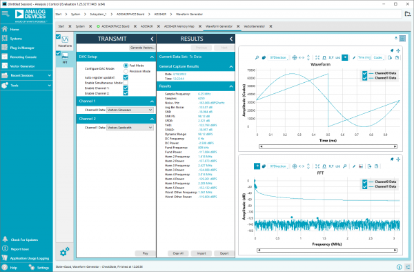
Figure 9. Waveform Generator View
The operation mode of AD3542R and the assignment of the waveforms is controlled from the Transmit pane that contains the following controls:
- Generate Vectors: this button opens the Vector Generator view there waveforms can be defined, scaled, loaded or exported. The use of this generator is covered in section Vector Generator View.
- DAC Mode: radio buttons allow selecting Fast Mode that uses 16-bit data or Precision Mode that uses 24-bit data. The same mode is used for both DAC channels when operated simultaneously.
- Auto Register Update: this feature automatically configures the interface registers to operate in streaming mode with the highest possible update rate. If this box is not checked, configuration must be made manually on the Memory Map. The settings are described at the end of this section.
- Enable Simultaneous Mode: this checkbox allows playing the same samples on both channels. Data is written to the DAC Page register, therefore maintaining the same update rate as for a single channel. When this box is checked, the waveform is selected in the Simultaneous Update menu as seen in Figure 10.
- Enable Channel 1/2: these checkboxes allow enabling channels individually. When both channels are enabled, each one can play a different waveform, as seen in Figure 11. The update rate depends on the DAC Mode and the update mode; all the combinations are shown in Table 8.
- Play Button: this button starts and stops the waveform playback. The status of the playback is displayed on the EVALAD3542R LED: blue when running and green when stopped.
Table 8. Update Rate Combinations
| Fast Mode (16 bit) | Precision Mode (24 bit) | |
|---|---|---|
| Dual Channel Mode | 6.25 MUPS | 4.16 MUPS |
| Single Channel / Simultaneous Mode | 12.5 MUPS | 8.33 MUPS |
![]()
Figure 10. Waveform Generation in Dual Mode
![]()
Figure 11. Waveform Generation in Simultanoeus Mode
Manual Register Configuration for Streaming Mode
If the Auto Register Update checkbox is not checked, the streaming mode parameters have to be configured manually in the memory map before pressing the Play button. The following registers must be set:
- STREAM_MODE register (0x0E). Length value should be set according to Table 9.
- TRANSFER_REGISTER (0x0F). Set STREAM_LENGTH_KEEP_VALUE bit to 1.
- INTERFACE_CONFIG_D register (0x14). Set SPI_CONFIG_DDR bit to 1.
Table 9. Stream Mode Length Values
| Fast Mode (16 bit) | Precision Mode (24 bit) | |
|---|---|---|
| Single Channel / Simultaneous Mode | 2 | 3 |
| Dual Channel Mode | 4 | 6 |
Vector Generator View
The Vector Generator view allows defining or loading waveforms that can later be assigned to the DAC channels. Waveforms are identified by name. The generator automatically adapts the sample rate based on the operating mode and the number of DAC channels enabled. A snapshot of this view if presented in Figure 12.
The Vector Generator tool is composed of the following sections:
- Predefined Waveforms. The generator has several predefined waveforms: DC, single tone, square, triangle, sawtooth, chirp, noise and multi-tone. Clicking the + button adds this waveform to the Generate panel where it can be customized.
- Waveforms from File. The generator can load waveforms from file in three different formats: text file, hexadecimal file or ACE Vector file. Refer to the ACE User Manual for further details on the file formats. When loading a waveform all the samples are played irrespective of the update rate. Therefor the waveform files must be generated for a specific update rate.
- First Waveform Parameters. Every waveform has a set of parameters that can be customized:
- Vector Name: specify a name in this field to identify the waveforms in the Waveform Generator view.
- Desired Frequency: specify the repetition frequency of the waveform. The value is assumed to be in Hz if no unit is specified. If the unit is specified, it must adhere to the standard capitalization (e.g. kHz, not khz).
- Attenuation: all waveforms are generated at full scale by default. Attenuation can be used to reduce the signal amplitude keeping the offset constant at mid scale. Amplitude is scaled by 10−Att 20.
- Relative Phase: specify the phase offset relative to the start of the waveform record.
- Preview button: pressing this button displays the waveform in the time-domain and its FFT in the frequency-domain window, if present.
- Copy: pressing this button duplicates the waveform entry in the Generate pane.
- Export: pressing this button allows exporting the waveform as a text file containing decimal numbers.
- Second Waveform Parameters. If a second waveform is added, it will show up stacked in the Generate pane under the first waveform. The same parameters are applicable.
- Time-domain waveform preview. A preview of the selected waveform is displayed in this window. Only one waveform is displayed at a time. The plot window allows zooming, panning and measuring on the waveform.
- Waveform FFT. The frequency-domain analysis of the selected waveform is displayed in this window. The plot window allows zooming, panning and measuring on the spectrum.

Figure 12. Vector Generator View
Creating a Waveform
Follow these steps to produce a dual waveform playback on the EVAL-AD3542R evaluation board:
- From the start page, double click on the board icon to open the Board view.
- Double click on the AD3542R block to open the Chip View.
- Click the button Proceed to Memory Map to open the Memory Map View.
- Go to CH0_CH1_OUTPUT_RANGE register and set the desired output range (0x33 in this example). Refer to Table 6 for the possible values of this register. Then click Apply All to force the register update.
- Click on the Vector Generator item on the left-hand panel to open the Vector Generator View.
- Follow the instructions given in Vector Generator View to create a 1 kHz sinewave and a 1 kHz sawtooth.
- Follow the shortcuts in the gray bar at the top of the window to go back to the Chip View. Then click on the button Proceed to Waveform Generator to open the Waveform Generator View.
- Select Fast Mode and enable channels 1 and 2. Then unfold the Channel 1 and Channel 2 sections to select each of the waveforms you created. Finally click the Play button.
- The LED on EVAL-AD3542R changes from green to blue and the playback starts. The waveforms should look like the ones shown in Figure 13 in the oscilloscope.

Figure 13. Dual Waveform Output
Unsupported Features in the Plugin
The current version of EVAL-AD3542R ACE Plugin (1.2021.38200) does not support all the board features at the moment. ACE notifies when an update of the plugin is available, so these features will be progressively incorporated. These are the features not currently supported:
- DAC output range selection and customization.
- CRC checking.
- Amplitude and offset control in waveform generation. Waveform scaling is only possible using the Attenuation field in dB. Offset is fixed to mid-scale.
- Using the LDAC line to update the DAC output.
- ALERT pin monitoring, error status readback and on-screen reporting.
- External clock for FPGA.
- External triggering of waveform playback.
Schematic, PCB Layout, Bill of Materials
resources/eval/user-guides/dac/eval-ad3542r.1647623518.txt.gz · Last modified: 18 Mar 2022 18:11 by Antonio Jimenez de Parga