


This version (06 Feb 2021 21:01) was approved by Robin Getz.The Previously approved version (14 Jan 2021 05:12) is available.
Table of Contents
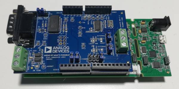
CN0401 (EVAL-ADM3055E-ARDZ) Shield Overview
CN0401 is an Arduino Uno compatible isolated controller area network with flexible data rate (CAN FD) communications port. The circuit interfaces to the local development platform via Serial Peripheral Interface (SPI) providing a simple method to add field bus communication to new and existing designs. CN0401 enables both the higher bandwidth CAN FD data rates (up to 8Mbps) demanded by modern multi-node CAN FD networks and the rugged electromagnetic compatibility (EMC) performance required by industrial environments.
The circuit uses the integrated auxiliary isolated digital channel of the ADM3055E transceiver for runtime configuration of the bus termination. The switchable termination circuitry connects a 120 Ω split termination with common-mode filtering capacitor between the CAN FD bus lines. Switchable termination allows on-the-fly software configuration of termination locations when the CAN FD bus is physically altered. Using switchable termination, each node can be used at any physical location without mechanical changes to the nodes and software can track the position of terminations in the network.
Additionally, the circuit can be set by the development platform to a reduced power standby state. While in the standby state, the isolated CAN FD communications port will notify the development platform of a remote wake-up request being transmitted by a remote CAN FD node to the CAN FD bus.
With the ADM3055E CAN FD transceiver, the circuit provides reinforced signal and power isolation between the node and CAN FD bus. Electrical connection to the CAN FD bus may be made either by screw terminal or the CAN CiA 303-1 male 9-pin sub-D port. Because the ADM3055E transceiver has an integrated isolated dc-to-dc converter, it does not require external power to be present on the CAN FD bus. The examples focus on CAN FD networks however this circuit is backwards compatible with classical CAN networks.
Hardware Connection and Jumper Configurations
The CN0401 connects to the ADICUP3029 or any Arduino Uno form-factor development platform using the mating headers. Shown below are the hardware connections and jumper headers which configure the operation of the board.

There should always be a shunt in jumper headers P2, P11, P19 and P20 for the board to function properly
Power Supply Connections and Configuration
The required power supply sources for both the logic and dc-to-dc converter can be independently configured via P20 and P11 jumpers to source power from either the underlying development platform or external power supplies.
P6 External Supply Terminal Block Pin Assignment
| Pin | Description |
|---|---|
| 1 | External DC-to-DC Converter Supply (5V) |
| 2 | External Logic Supply (2.7V to 5.5V) |
| 3 | Ground |
P20 Header Shunt Positions for Setting Board Power Source
| Position | Location | Description |
|---|---|---|
| Shunt pins 1 and 2 |  | Board sources the required supply for the isolated dc-to-dc converter from the 5V Arduino Uno header pin |
| Shunt pins 2 and 3 |  | Board sources the required supply for the isolated dc-to-dc converter from the External Supply Terminal Block (P6-Pin 1) |
P11 Header Shunt Positions for Setting Board Voltage Logic
| Position | Location | Description |
|---|---|---|
| Shunt pins 1 and 2 |  | Board sources the logic supply from the IOREF Arduino Uno Header Pin |
| Shunt pins 2 and 3 |  | Board sources the logic supply from the External Supply Terminal Block (P6-Pin 2). The logic levels will scale with the supply voltage and typically must match the level of the development platform. |
CAN Bus Connections
The board can be connected to the CAN bus via the CAN bus terminal block or the standard CAN port: CiA 303-1 male 9-pin sub-D port.
CAN Bus Terminal Block Pin Assignment
| Pin | Description |
|---|---|
| 1 | CANL |
| 2 | CANH |
| 3 | GND2 |
CiA 303-1 Male 9-pin Sub-D Port
| Pin | Description |
|---|---|
| 1 | Not Connected |
| 2 | CANL |
| 3 | GND2 |
| 4 | Not Connected |
| 5 | Not Connected (Optionally can be configured to GND2 via R2) |
| 6 | Not Connected (Optionally can be configured to GND2 via R4) |
| 7 | CANH |
| 8 | Not Connected |
| 9 | Not Connected |
SPI Interface Chip Select Pin Configuration
The board's SPI Interface has a configurable pin assignment for its chip select to support multiple shield stack-up on the same development platform. The chip select signal can be routed to one of four different Arduino pins via mechanical shunt on the P2 header.
P2 Header Shunt Positions for Setting SPI Chip Select Pin
| Position | Location | Description |
|---|---|---|
| Shunt pins 1 and 2 |  | Board uses Arduino pin D10 as chip select |
| Shunt pins 3 and 4 |  | Board uses Arduino pin D9 as chip select |
| Shunt pins 5 and 6 |  | Board uses Arduino pin D8 as chip select |
| Shunt pins 7 and 8 |  | Board uses Arduino pin D7 as chip select |
Silent Mode and Interrupt Configuration
Silent mode of ADM3055E transceiver is accessible to the development platform through the Arduino Uno D4 header pin. The CAN FD controller issues service requests to the development platform as interrupts through the mechanical shunt on P7.
P5 and P7 Shunt Placement
| Jumper Header | Location | Description |
|---|---|---|
| P5 |  | With the mechanical shunt on P5 installed, the development platform can set the CAN FD transceiver to silent mode via high signal from the Arduino Uno header pin D4. Silent mode allows normal reception of CAN frames, but disallows transmission to the CAN bus of any output from the CAN controller. Control of this signal is not required for normal operation. The transceiver will function normally with the mechanical shunt on P5 removed. |
| P7 |  | The development platform will receive service requests from the CAN controller via Arduino Uno header pin D2. The mechanical shunt on P7 must be in place to detect received CAN frames and notification that the remote wake-up pattern has been received. This shunt will typically be left in place, and is provided only in case the interrupt signal must be routed to a different development platform input. |
Slope Control and Full Speed Mode
The ADM3055E can be set to full speed mode, slope control mode or standby mode via mechanical shunt position P19. In full-speed mode, the transition times of the signal transmitted to the CAN bus supports all data rates up to the maximum data rate. In slope control mode, the slew rate of the CAN bus lines is decreased to reduce emissions from fast edges and will only be used for lower data rates. If the mechanical shunt on P19 is removed and the RS signal allowed to float, the transceiver will enter standby mode.
P19 Shunt Position for Setting Slope Control and Full Speed Mode
| Position | Location | Description |
|---|---|---|
| Shunt pins 1 and 2 |  | The ADM3055E transceiver is set to full speed mode |
| Shunt pins 2 and 3 |  | The ADM3055E transceiver is set to slope control mode |
Software
Schematic, PCB Layout, Bill of Materials
CN0401 Design & Integration Files
- Schematics
- PCB Layout
- Bill of Materials
- Allegro Project
End of Document
resources/eval/user-guides/circuits-from-the-lab/cn0401.txt · Last modified: 06 Feb 2021 21:01 by Robin Getz