


This version is outdated by a newer approved version. This version (13 Jun 2017 12:14) is a draft.
Approvals: 0/1The Previously approved version (23 Jul 2014 13:55) is available.
This version (13 Jun 2017 12:14) is a draft.Approvals: 0/1The Previously approved version (23 Jul 2014 13:55) is available.
This is an old revision of the document!
Table of Contents
CN0349 Software User Guide
Overview
CN0349 provides robust and complete solution for processing conductivity and temperature inputs into digital code. The design solution is optimized for high precision and low cost measurement, using five active devices, and has a total error less than 1% FSR after calibration. The output of the circuit is fully isolated, and therefore, the ground-loop interference is effectively reduced, making it ideal for industrial applications.
The circuit shown in Figure 1 incorporates the AD5934YRSZ 12 bit Impedance Converter, ADG715BRUZ Octal SPST Switch, AD8606ARZ Rail-to-Rail OpAmp, ADuM5000ARWZ Isolated DC-DC Converter, ADuM1250ARZ Dual I2C Isolator, to convert the conductivity and temperature inputs to digital code.
The circuit has 8pin Digilent Pmod I2C interface connector on board, which could be used for connection to a customer microprocessor or FPGA.
The CN0349 circuit note discusses the design steps needed to optimize the circuit shown in Figure 1 for a specific measuring range including accuracy analysis and component selection considerations.
The performance of the circuit could be demonstrated with the use of Analog Devices SDP controller EVAL-SDP-CB1Z and SDP-to-PMOD Interposer Board SDP-PMD-IB1Z, both optional purchase items.
This user guide discusses the use of the evaluation software to collect data from the EVAL-CN0349-PMDZ Evaluation Board CN0349

Figure 1. Data Acquisition system for conductivity measurements with isolation (All connections and Decoupling Not Shown)
Required Equipment
- EVAL-SDP-CB1Z Controller Board (SDP-B Board)
- EVAL-CN0349-PMDZ Evaluation Board (CN-0349 Board)
- EVAL-CFTL-6V-PWRZ (+6V Power Supply) or equivalent
- http://www.analog.com/SDP-PMD-IB1Z SDP-to-PMOD interposer board
- Resistance Decade Box (to simulate the input impedance, e.g. IET RS-200 Labs Resistance Substituter Decade Box) or real conductivity cell with integrated Pt100 sensor (e.g. Sensorex CS200TC-PT1)
- (supplied with provided CD in kit)
- PC with the following Minimum Requirements
- Windows XP Service Pack 2 (32-bit)
- USB type A Port
- Processor rated at 1GHz or faster
- 512 MB RAM and 500 MB available hard disk space
- USB type A to USB type mini-B cable (provided with the EVAL-SDP-CB1Z Controller Board)
General Setup
- The EVAL-CFTL-6V-PWRZ (+6V DC Power Supply) powers the SDP-PMD-IB1Z (Interposer Board) via the DC barrel jack.
- The SDP-PMD-IB1Z (Interposer Board) connects to the EVAL-SDP-CB1Z (SDP-B Board) via the 120-Pin connector A.
- The EVAL-SDP-CB1Z (SDP-B Board) connects to the PC via the USB cable.
- The EVAL-CN0349-PMDZ (CN0349) connects to the EVAL-PMD-IB1Z (Interposer board) via the 8-pin header Digilent Pmod I2C interface connectors (J2 on both boards). Use the 4-pin MTE Cable (Digilent, Inc.) supplied with CN0349 board.
- The resistance decade box/the conductivity cell connects to the EVAL-CN0349-PMDZ (CN0349 Board) via the terminal block J1

Installing the Software
- Load the evaluation software by placing the CN0349 evaluation software disc in the CD drive of the PC. You can also download the most up to date copy of the evaluation software from www.analog.com/CN0349. Open the file setup.exe.
NOTE: It is recommended that you install the CN0349 Evaluation Software to the default directory path C:\Program Files\Analog Devices\CN0349\ and all National Instruments products to C:\Program Files\National Instruments\

- Click Next to view the installation review page

- Click Next to start the installation

- Upon completion of the installation of the CN0349 Evaluation Software, the installer for the ADI SDP Drivers will execute.
NOTE: It is recommended that you close all other applications before clicking “Next”. This will make it possible to update relevant system files without having to reboot your computer.
\\
- Press “Next” to set the installation location for the SDP Drivers.
It is recommended that you install the drivers to the default directory path
C:\Program Files\Analog Devices\SDP\DriversR2

- Press “Next” to install the SDP Drivers and complete the installation of all software. Click “Finish” when done.

—-
Connecting the Hardware
- Connect the +6V DC Power Supply (Wallwart) to the barrel jack J1 of the Interposer Board (Interposer Board ) as depicted below.
NOTE: Make sure that the jumper is positioned as shown below!

- Connect the 120-pin connector on the SDP-PMD-IB1Z (Interposer Board) to the 120-pin connector marked “CON A” on the EVAL-SDP-CB1Z (SDP-B Board)
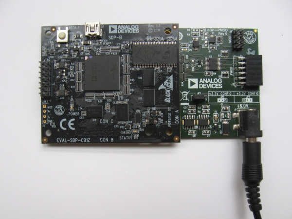
- Connect the USB cable supplied with EVAL-SDP-CB1Z (SDP-B Board) to the USB port on the PC and the SDP Board
 }}
}}
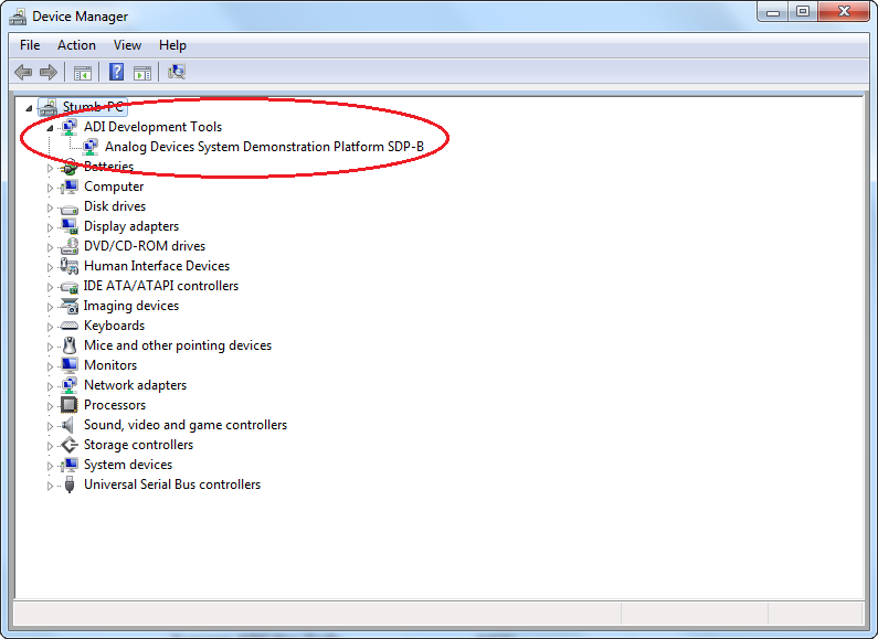
NOTE: Verify that the SDP Drivers are loaded properly. For that purpose open the Device manager and check if the SDP Board is recognized. If not repeat steps 1-3
- Connect the EVAL-CN0349-PMDZ (CN0349 Board) to the SDP-PMD-IB1Z (Interposer Board) via the 8 pin header Digilent Pmod I2C interface connector.

- Connect the Resistance Decade Box/Conductivity Cell to pin4 and pin5 of J1 Terminal Block located on EVAL-CN0349-PMDZ (CN0349 Board). If a Conductivity Cell with integrated Pt100 sensor is used, the sensor should be wired to pin 3 and pin 2 of J1 Terminal Block. Pin 1 can be used to wire the ground shield of the Conductivity Cell.
- After a proper connection of the hardware to the PC the CN0349 Evaluation Software can be used to calibrate the board and capture data.


Using the Evaluation Software
Software Control and Indicator Descriptions


\\
- Measure Button
- When this button is pressed, the SDP-B Board will perform a measurement procedure and present the data in the measurement data indicators (3,4,5,6).
- Control Tabs
- Main - Clicking this tab brings the data collection graph to the front.
- Calibrate System - Clicking this tab brings the system calibration settings to the front.
- SDP Revision - Clicking this tab brings the SDP board information window to the front.
- Impedance Indicator
- This indicator displays the measured input impedance in Ω).
- Conductivity Indicator
- This indicator displays the measured input conductivity in mS/cm. The measurement result is dependent on the applied probe corrections (7) and (9).
- Conductivity Temperature Compensated Indicator
- This indicator displays the temperature compensated input conductivity in mS/cm according to the chosen Temperature coefficient (8)
- Temperature of the Solution Indicator
- This indicator displays the measured temperature in °C, using external Pt100 RTD sensor
- Cell Constant Control (Probe Corrections)
- This control is used to apply the constant of the cell used for the measurement. The value of this control affects the measurement result presented in the Conductivity Indicator (4).
- Temperature Coefficient Control (Probe Corrections)
- This control is used to apply the temperature coefficient of the measured solution.
- Offset Control (Probe Corrections)
- This control is used to apply offset correction to the measured Conductivity (4). If offset correction is not needed, leave this control at 0mS/cm.
- Measurement Range Radio Buttons
- This control determines the input measurement range. The two measurement ranges are.
- Measurement Range Indicator
- This indicator shows the limits of the chosen input measurement range.
- System Status String Indicator
- This indicator displays a message to the user detailing the current state of the software.
- System Status LED Indicator
- This indicator displays the current state of the software in the form of an LED. There are four status LED colors.
 Inactive
 Busy
Busy
 Error
Error
 Waiting for user action
- Calibrate Button
- Pressing this button initiates a calibration of the board.
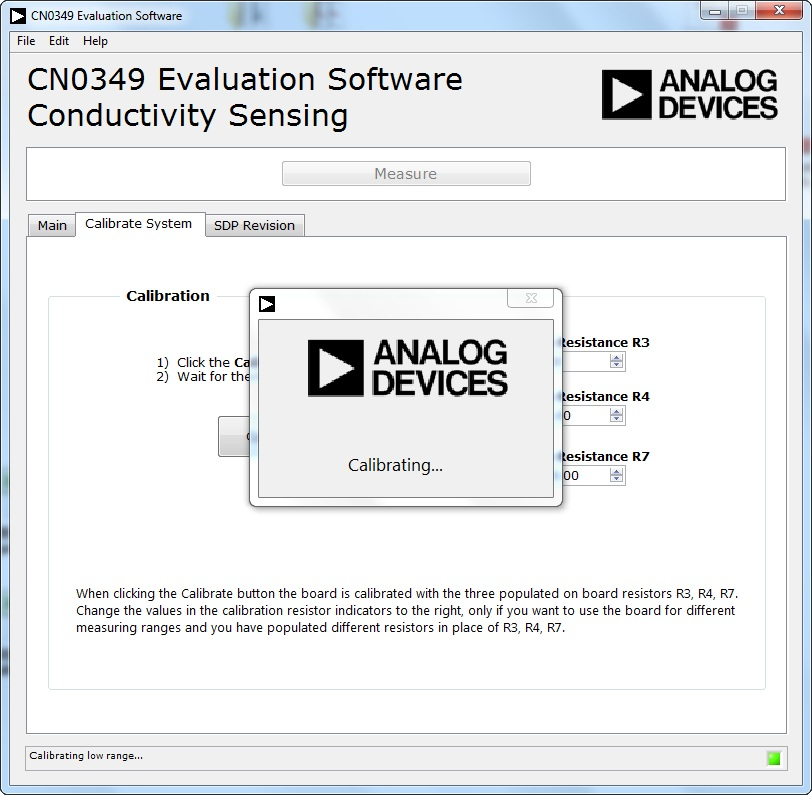
- Calibration Resistances Controls
- This control is used to apply the values for the three on board calibration resistances R3, R4, R7. The values for this controls has to be changed only if different calibration resistances are populated on the board.
- SDP Firmware Revision
- Read only data. After the connection is established with the SDP Board, the basic information for the controller can be found here.
Establishing a USB Connection Link
- Follow the instructions to properly install the software and connect the hardware as described in the previous sections.
- Open the file named CN0349.exe in the installation directory or the shortcut in the start menu.
NOTE: If the software was installed to the default location it will be found at
C:\Program Files\Analog Devices\CN0349\CN0349.exe
- The software should connect to the board automatically. If the hardware is not recognized by the PC the next window will appear, indicating that the software is waiting for proper hardware connection. If that happens perform the hardware connection procedure described in the previous section. After connecting the hardware the list in the window will populate. Choose the connected hardware and click select.

- Upon success, the System Status String Indicator will display SDP Board Ready to Acquire Data
Calibrating the CN0349 Board
Calibration Procedure Steps
- Establish a USB Connection Link.
- Click the Calibrate System tab.
- Press the Calibrate Button.
- A pop-up window will appear indicating that the board is being calibrated. Wait for the calibration to finish.
- When the calibration is finished a second pop-up window will appear to indicate the end of the measurement. Click the OK button.

Measuring Data
- Establish a USB Connection Link.
- Choose the appropriate Probe Corrections .
- Choose the Measurement Range .
- Click the Measure button .
- A pop-up window appear to indicate that the board is performing a measurement procedure.
- When the measurement is finished a second pop-up window will appear to indicate the end of the measurement. Click the OK button to close the pop-up window.
- After clicking OK the indicators are presenting the measured data.
Use the CN0349 with customer own platform
This Chapter will describe how to use the CN0349 board with a customer platform other than the SDP-B platform. In this section we refer to customer platform the “host”. The host can be a MCU platform, FPGA platform, or PC with USB to I2C converter, or any type of programmable platform which has an I2C interface.
Hardware interface of CN0349
For the detailed specifications of the I2C interface, please check: I2C-bus specification. Notice that the CN0349 board does not support all the feastures of the I2C-bus specification, and the limitations will described later.
The EVAL-CN0349-PMDZ evaluation board uses a standard Dignlent Pmod 8pin I2C connector interface, J2, to communicate with the host. For the detailed Digilent Pmod interface specification please check: Digilent Pmod Interface Specification
The CN0349 board can accept both +3.3V±10% or +5V±10% power supplies. Please make sure the host has the same I/O level standard as the CN0349 board. The power supply for the CN0349 board minimum current requirement is 300mA. The power supply for CN0349 must provide this current with minimum voltage drop. Otherwise the permanent damage of CN0349 may occur.
Software interface for CN0349
For the customer platform to communicate with the CN0349 board, the I2C communication protocol must be designed carefully. The maximum I2C speed and timing is limited by the ADG715 and the AD5934. Please check the data sheet for the AD5934 and ADG715 for more specific details. The host I2C timing and speed must meet with the requirements of both the ADG715 and AD5934. The maximum I2C clock speed for ADG715 and AD5934 is 400kHz.
Caution: In the EVAL-CN0394-PMDZ evaluation board, the ADG715 I2C address is set to: 0x48, and the AD5934 I2C address is: 0x0d. Please make sure in the host I2C bus there are no devices that have same address as the ADG715 and AD5934.
In the host software the AD5934 following settings must be observed, otherwise the results may incorrect:
- Address 0x80 control register value: 0x01 (the excitation voltage 2.0Vpp, PGA=1)
In the host software the ADG715 register must be set to one of following conditions, otherwise incorrect results may occur:
- 0x09, calibrate for RFB=R9=100Ω, RCAL=R3=100Ω
- 0x11, calibrate for RFB=R9=100Ω, RCAL=R4=1kΩ
- 0x12, calibrate for RFB=R8=1kΩ, RCAL=R4=1kΩ
- 0x22, calibrate for RFB=R8=1kΩ, RCAL=R7=10kΩ
- 0x41, measure RTD with RFB=R9=100Ω
- 0x81, measure YX with RFB=R9=100Ω
- 0x82, measure YX with RFB=R8=1kΩ
The CN0349 board must be calibrated before measurement. The calibrations theory and calculations are located in circuit note CN0349.
The following shows the two allowable ranges for the conductivity cell admittance. If the conductivity cell admittance is out of these ranges, incorrect results may occur. Please note: the admittance of the cell is not the conductivity of the cell, the cell constant must be used to convert the admittance to conductivity. For the details of the cell constant please check circuit note CN0349.
- low range: 1uS~1mS, calibrate with item 3 and 4, measured with item 7 (see above)
- high range: 1mS~1S calibrate with item 1 and 2 measured with item 6 (see above)
Please note that the measurement result is the YX not YCELL. the details of converting YX to YCELL are give in CN0349.
The hardware limitations in the CN0349 board need to be considered carefully. If other settings for AD5934 and ADG715 outside the limits described above are used, the AD5934 ADC input must not be saturated. The AD5934 ADC reference is AVDD2=3.3V which determines the input range. The AD5934 ADC input signal amplitude is a function of the excitation voltage, the RC filter made up of R1, R5, C1, the ADG715 setting, the admittance of conductivity cell, and the AD5934 internal PGA gain settings. Incorrect results will be obtained if any of these factors cause the AD5934 ADC input signal to go out of range.
resources/eval/user-guides/circuits-from-the-lab/cn0349.1497348845.txt.gz · Last modified: 13 Jun 2017 12:14 by Robert Lee