


This version is outdated by a newer approved version. This version (17 Jan 2023 13:28) was approved by Mark Bolger.The Previously approved version (19 Nov 2021 11:31) is available.
This version (17 Jan 2023 13:28) was approved by Mark Bolger.The Previously approved version (19 Nov 2021 11:31) is available.This is an old revision of the document!
Table of Contents
PHY Exchange Guide, KSZ8081RNB/MNX to ADIN1200 10/100Mb
Overview
This PHY exchange guide captures pertinent information to support migration from the MicroChip KSZ8081MNX/RNB to the Analog Devices ADIN1200 Ethernet PHY. The ADIN1200 supports MII, RMII and RGMII MAC interfaces from the same package version, while the KZS8081MNX version supports a MII MAC interface and the KSZ8081RNB supports RMII. The PHYs have different pinouts, therefore the ADIN1200 is not a drop-in replacement for the Microchip product. This requires edits to the schematic and board layout to achieve this exchange. The following sections detail the modifications at the schematic level required to migrate from KSZ8081 to the ADIN1200 device.
Hardware Changes By Function
Power Supplies Overview
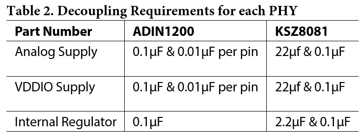
The supply requirements are listed in Table 1. Both devices can operate from a minimum of one 3.3V power supply rail AVDD_3P3 (VDDA_3.3V), where the VDDIO rail is connected to 3.3V. Both devices have an on chip voltage regulator to generate the internal core supply rail and provided to a pin for decoupling purposes.

The ADIN1200 is robust to power supply sequencing and the power can be applied in any order. The ADIN1200 provides two pins for each supply rail, whereas the Microchip device provides one power supply pin for each rail. The VDDIO supply rail powers the MAC interface and MDIO blocks, this can operate from 1.8V, 2.5V or 3.3V. Decoupling requirements for each device differs as described in Table 2
RESET Operation
An active low hardware reset pin, RESET_N (RST#) is provided on Pin 6 of the ADIN1200 and pin 32 of the KSZ8081. The hardware strapping pins are read and updated at the de-assertion of reset for both devices. For the ADIN1200, the RESET_N pin resides in the AVDD_3P3 voltage domain, whereas for the Microchip device, the RST# pin is referenced to VDDIO. In applications where the MAC interface is powered from VDDIO of 1.8V, level shifting of the RESET_N signal applied to the ADIN1200 may be required to ensure the voltage level on the RESET_N pin is in excess of the minimum input high threshold level.
Clocking
A 25 MHz crystal or external clock source is used to provide the reference clock for both devices. In RMII mode, the ADIN1200 expects an external 50MHz REF_CLK provided to the XTAL_I/REF_CLK pin. The KSZ8081RNB (RMII mode) can provide a 50 MHz REF_CLK to the MAC device from the 25 MHz source. Alternatively, an external 50 MHz clock can be provided to both the PHY and MAC.
Bias Resistor
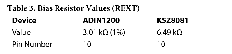
An external resistor, REXT is required to bias internal reference circuitry for both KSZ8081 and ADIN1200. The ADIN1200 requires a 3.01 kΩ resistor (1% tolerance, 100 ppm/°C temperature coefficient) connected to pin 10. The KSZ8081 uses an 6.49 kΩ on pin 10.
Media Dependent Interface (MDI)
The ADIN1200 has voltage mode line drivers with on-chip terminations so no external termination resistors are required and the center tap of the transformer does not require biasing to supply voltage. Both devices use voltage mode line drive for connection from the MDI_0:1_P/N (RXM/P, TXM/P) pins to the magnetics and RJ-45 line using the same external circuit.
The recommended external circuit for the interface to the magnetics and RJ-45 is shown in Figure 1.
The KSZ8081 is also a voltage mode PHY.
 Figure 1 Isolation using Discrete Magnetics
MDIO/Management Interface
Both devices can be hardware strapped to be used in an unmanaged configuration. Alternatively, they can provide SMI/MII access over the two wire MDIO interface. The MDIO pin (Management Data Open Drain Input/Output) for SMI/MII interface to MAC and requires an external pullup resistor. The recommended value for ADIN1200 is a 1.5kΩ resistor connected to pin 24. The KSZ8081 recommends 1kΩ connected to pin 11. A hardware interrupt output pin INT_N (INTRP) is provided in both devices and is open drain. The recommended value for ADIN1200 is a 1.5kΩ resistor connected to INT_N pin 27. The KSZ8081 recommends 1kΩ connected to INTRP, pin 21.
LED Function
Both devices support two LED pins. The ADIN1200 pins are LED_0 and LINK_ST. The LED_0 has programmability of LED functions, with different blinking operation possible through MDIO configuration, the default mode is ON when Link is Up, blink if activity. The LINK_ST provides static information about Link up or down status. The KSZ8081 pins are LED0, LED1, where LED0 can be configured for On/Off and Blink if activity while LED1 can be configured to indicate 10 or 100M link speed. Both devices use these pins for Speed and Auto-Neg strapping purposes.
LED Circuit
The ADIN1200 LED_0 operates from the AVDD_3P3 voltage domain, therefore can support driving LEDs even when the MAC interface is running at the lower voltage of 1.8V. The KSZ8081 LED circuits operate from the VDDIO domain.
The default LED operation is on if the Link is up and blinks when there is activity, this operation can be reprogrammed through MDIO write.
For the LED_0 of the ADIN1200, it can be configured with 4-level strapping. The strapping configuration will have an impact on how the LED function operates, and needs to be considered if the LED pins are used to directly drive an LED. If the strap pin is pulled high by the strapping resistors, (MODE_3/MODE_4) the output will be configured as an active low driver and conversely if the strapping input is pulled low (MODE_0/MODE_1), the output will be configured as active high. This LED circuit should be configured accordingly.
 Figure 2. LED_0 Hardware Configuration Pin Interaction
Link Status, LINK_ST
The ADIN1200 has a dedicated LINK_ST pin to provide information to the MAC on the status of the Link. By default, the LINK_ST pin goes high indicating the link is up and low to indicate the link is down. The LINK_ST polarity is programmable by setting the bit high GE_LNK_STAT_INV_EN. The LINK_ST could be used to drive an LED, however it resides in the VDDIO voltage domain, therefore, when driving an LED in an integrated RJ45 jack where the PHY VDDIO is 1.8V, level shifting will be required.
MAC Interface
The ADIN1200 supports MII, RMII and RGMII MAC interface modes, whereas the KSZ8081RNB supports RMII and the KSZ8081MNX supports MII interface. The following sections describe specifically the MII and RMII interfaces for both devices.
MII Interface
The MII interface is the communication path between the PHY and MAC devices. The KSZ8081MNX version will be covered here. The MII interface has a high pin count, with a total of 15 pins for data transmission, reception and to signal errors or collision. It is sometimes used in 100M applications as it has a lower latency than RGMII and is much lower than RMII. Table 4 shows a pin overview of both devices for the MII MAC interface mode. When using the ADIN1200 in MII mode, the multifunction pin “LED_0/COL/TX_ER” automatically becomes COL. Similarly, the “INT_N/CRS” becomes CRS. The ADIN1200 sub-system registers provide user with ability to reconfigure which pin the COL and CRS functions are provided on (option of redirecting to GP_CLK, LINK_ST or INT_N). This requires a register write over MDIO interface to reconfigure.

RMII Interface
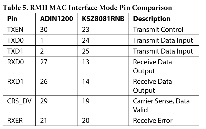
The KSZ8081RNB model has RMII interface. RMII is a reduced MII interface using fewer pins as shown in Table 5. The pin count for this interface is 8 pins.
RMII mode requires a 50MHz clock, REF_CLK. The KSZ8081RNB can generate a 50MHz clock internally and provide it to the MAC. Alternatively, it can accept an external 50MHz clock from the MAC. In RMII mode, the ADIN1200 requires an external 50MHz clock applied to XTAL_I.
RGMII Interface
The ADIN1200 supports an RGMII interface mode, while the KSZ8081 does not. The RGMII interface has a low pin count interface support for 10M, 100M and Gigabit operation with a total of 12 pins for data transmission, reception and to signal errors or collisions. It is the most common interface used for Gigabit applications. The ADIN1200 can support 10/100 M speeds over the RGMII interface. Table 6 shows a pin overview of the ADIN1200 RGMII interface.

Output Clocks
The ADIN1200 can optionally provide a number of clock signals on the GP_CLK pin. This is configured via MDIO writes and the clocks available are a 125 MHz free running clock, 25 MHz clock and 25MHz/125 MHz recovered clock.
Hardware Configuration
Both devices have a number of strapping options to enable managed or unmanaged configurations of the PHY function such as PHY address, mode of operation, Auto-Negotiation and MAC Interface.
After power on, the strapping pin voltages get sensed and latched upon existing from a reset and the sensed voltages are used to set the personality of the PHY.
When configuring any strapping configurations, ensure to review the default state of the MAC side, whether the pins are being driven when coming out of reset or if there are internal pulls. Understanding the behavior on the MAC side is key to ensuring there are no conflicts with the hardware strapping implemented, or to adjust the strapping resistor values if required.
The KSZ8081 uses 2-level strapping options throughout, while the ADIN1200 uses a mix of 2-level and 4-level. In general, strapping pins are multi-functional and have different operation after the device is brought out of reset. The ADIN1200 has internal pull downs on many of its strapping pins (not all), therefore it would be possible to minimize external strapping resistors.
 Figure 3. ADIN1200 Hardware Strapping, 2 and 4 level strapping resistors

Strapping configurations are very specific to the device, consult the respective datasheets to determine the exact configuration for required use case.
Hardware Configuration of Speed
For the ADIN1200, speed configuration is done using two pins, PHY_CFG0 and PHY_CFG1. These pins do not have any internal pull resistors, therefore external strapping is required. Both pins support 4-level strapping, providing much flexibility in terms of the possible combinations, such as Auto-neg speeds shown in Table 8 or Forced modes shown in Table 9. Review the datasheet hardware configuration pin section for full detail on the possible settings using these pins. The KSZ8081 uses pin SPEED to select between 10 or 100 M speeds and pin DUPLEX to configure HD or FD.


Hardware Configuration of Auto-MDIX
Selection of Auto-MDIX for the ADIN1200 is done using one pin, (MDIX_MODE) with 4-level strapping.
In the KSZ8081 Auto-MDI/MDI-X is enabled by default and can be disabled/configured with an MDIO write.

MAC Interface Selection
The ADIN1200 uses two hardware pins, MACIF_SEL0 and MACIF_SEL1 to provide user ability to select different MAC interfaces. These two pins have internal weak pull downs, therefore the default operation would be RGMII with delays as shown in Table 11. To configure any other MAC interface mode, use 10kΩ pull up or pull down resistors to select accordingly. The KSZ8081 MAC interface selection (RMII/MII) is chosen by selecting the appropriate part version (RNB/MNX).
Hardware Configuration of PHY Address
Both devices have a default strapping providing a PHY address of 0x0000. The ADIN1200 provides four PHY address pins, allowing up to 16 unique addresses possible. The PHY address pins are shared with the RXD output pins. The KSZ8081 provides three PHY address pins, capable of 8 unique addresses. Two PHY Address pins are dedicated pins, with the third PHY address shared with an RXD output pin. Both devices use two-level strapping, either pull high or low to configure the PHY address.
Strapping configurations are very specific to the device, consult the respective datasheets to determine the exact configuration for required use case.
Package
Both the ADIN1200 and the KSZ8081 are available in a 32 lead QFN/LFCSP package of 5 mm x 5mm body size. The devices have different pinouts, therefore the ADIN1200 is not a drop-in replacement for the Microchip product. This requires edits to the schematic and board layout to achieve this exchange.
The underside of the LFCSP package for the ADIN1200 includes an exposed paddle which should be soldered directly to the board with an array of vias for thermal purposes. There are also two exposed stripes adjacent to the exposed paddle. These do not need to be soldered to the board, they should be treated as a keepout area as they are connected to supply rails in the device, therefore should not be tied to ground and there should be no routing or traces on the PCB layer directly underneath them.
Other Pinout Considerations
Integrated MDI Termination
Both devices include integrated termination resistors on the MDI paths. These are voltage mode PHYs, no external resistors are required for biasing and no supply voltage is required at the center tap of the transformer.
RGMII
The ADIN1200 also supports RGMII MAC interface mode.
Software Considerations
Both devices can be hardware strapped to be used in an unmanaged configuration. Alternatively, they can provide SMI/MII access over the MDIO interface. The KSZ8081 supports Clause 22 register access, while the ADIN1200 supports both Clause 22 and Clause 45 access. Registers 0x0 to 0xF are common across all PHYs.
Linux Driver
The ADIN1200 has a Linux Driver available in the Linux mainline kernel. The ADIN1200 linux driver detail is captured here: https://wiki.analog.com/resources/tools-software/linux-drivers/net-phy/adin
The ADIN1200 has a Linux Driver available in the Linux mainline kernel.
High Level Comparison

Side by Side Package/Pinout Comparison
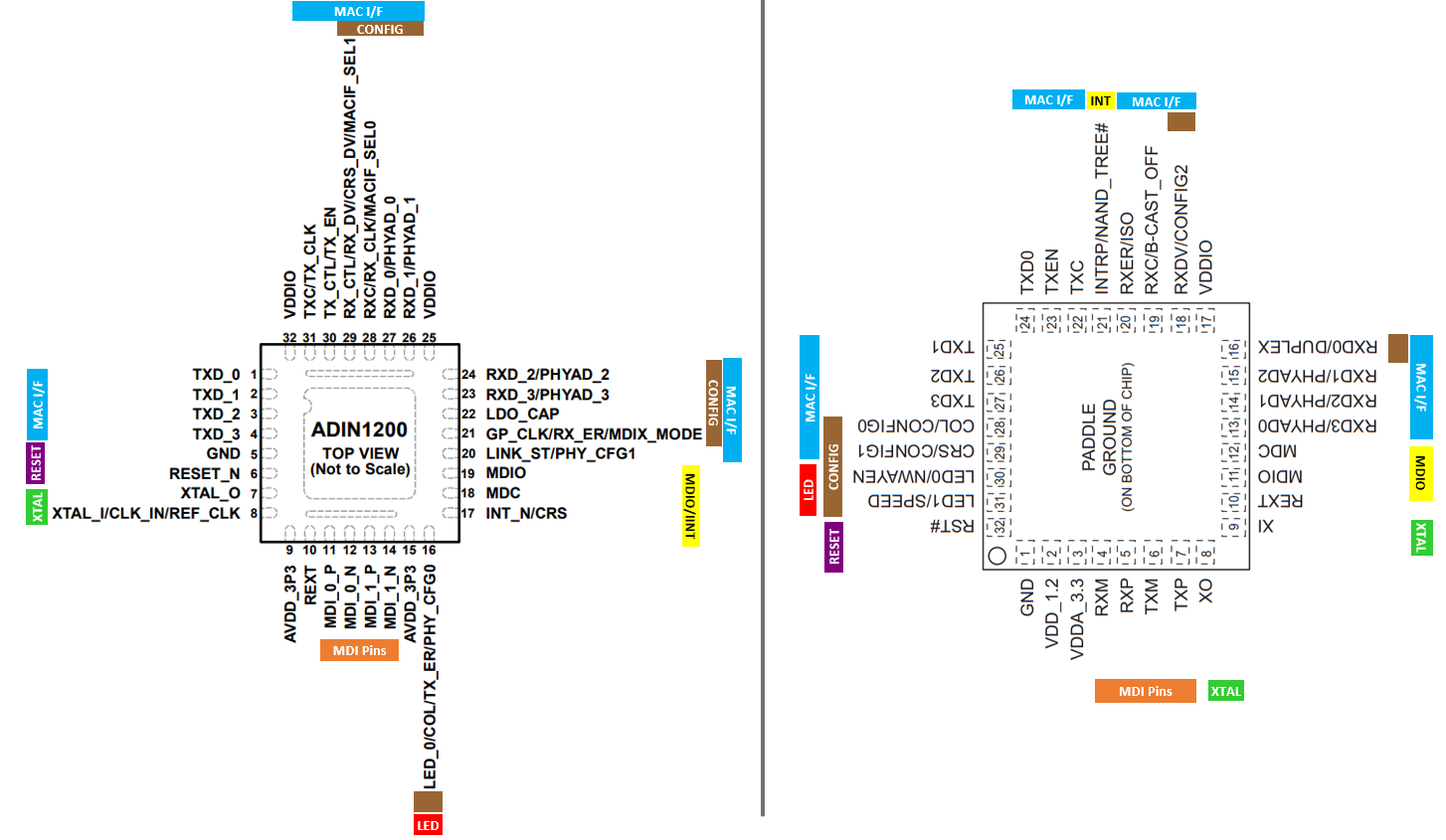
The following is a side-by-side comparison of the package and pinouts, showing the position of the corresponding functional pins on each device.
Example Configurations for RMII
The following example captures how to configure the ADIN1200 for an unmanaged configuration with RMII Interface, operating in Auto-negotiation mode advertising all speeds. The PHY will power up in this state, ready to establish a link with a link partner. The MAC interface configuration pins (MACIF_SEL0/1) are pulled to VDDIO, setting the PHY to RMII mode. GP_CLK is set to MODE_3 to configure an automatic MDIX operation. In addition, the PHY_CFG0 and PHY_CFG1 pins are configured for MODE_4 and MODE_1 respectively. The PHY_CFG0 pin is also shared with the LED_0 pin, it’s configuration with MODE_4 means an active low LED can be used on LED_0.
The following list summarizes an RMII auto negotiate, 10 Mbps or 100 Mbps full duplex or half duplex:
- MAC Interface = RMII
- MACIF_SEL0 = MODE_1 = 10 kΩ pull-up resistor
- MACIF_SEL1 = MODE_1 = 10 kΩ pull-up resistor
- MDIX_MODE = automatic MDIX, preferred MDIX
- MDIX_MODE = MODE_3
- PHY address = 0b0001
- Speed selection = 10 Mbps, 100 Mbps with full duplex or half duplex, auto-negotiation enabled
- PHY_CFG0 = MODE_4 = 10 kΩ pull-up resistor
- PHY_CFG1 = MODE_1 = 10 kΩ pull-down resistor

resources/eval/user-guides/adin1300-and-adin1200/ksz8081_to_adin1200_phy_exchange_guide.1673958520.txt.gz · Last modified: 17 Jan 2023 13:28 by Mark Bolger