


This version is outdated by a newer approved version. This version (28 Mar 2022 09:37) was approved by Adrian Costina.The Previously approved version (30 Sep 2021 14:43) is available.
This version (28 Mar 2022 09:37) was approved by Adrian Costina.The Previously approved version (30 Sep 2021 14:43) is available.This is an old revision of the document!
AD9213-DUAL-EBZ HDL reference design
Functional Overview
The AD9213-DUAL-EBZ reference design is a processor based (e.g. ARM) embedded system. The device interfaces to the FPGA transceivers followed by the individual JESD204B and ADC cores. The cores are programmable through an AXI-Lite interface. The samples are initially captured UTIL_ADC_FIFO and then passed to the system memory (DDR). The user can capture up to 1048576 samples per channel, if both channels are selected or 2097152 per channel if only one channel is selected or in the case the data is considered single channel interposed.
The reference design supports the following evaluation board:
| Hardware | Evaluation Document |
|---|---|
| DUAL-AD9213 | DUAL-AD9213 |
Supported Carriers
- Stratix10SOC FMC+ Slots
Building the HDL project
General build instructions can be found here: Building HDL
Block Diagram
The data path and clock domains are depicted on the below diagram:

The design has two JESD receive chains each having 16 lanes at rate of 12.5Gbps. The JESD receive chain consists of a physical layer represented by an XCVR module, a link layer represented by an RX JESD LINK module. The transport layer is common and is represented by a RX JESD TPL module. The links operate in Subclass 1 by using the SYSREF signal to edge align the internal local multiframe clock and to release the received data in the same moment from all lanes. Therefore ensuring that data from all channels is synchronized at the application layer.
Both links are set for full bandwidth mode and operate with the following parameters:
- Deframer paramaters: L=32, M=2, F=2, S=16, N’=16
- GLBLCLK – 312.5MHz (Lane Rate/40)
- REFCLK – 312.5 MHz (Lane Rate/20)
- SYSREF – 1.46MHz (DEVCLK/2048)
- DEVCLK – 10000MHz
- JESD204B Lane Rate – 12.5Gbps
The transport layer component present on the output 1024 bits at once on every clock cycle, representing 16 samples per converter. The typical AXI_PACK IP does not meet timing in this design, so a custom one was implemented in the system_top.v module. An ADC buffer is used to store 1024k samples per converter in the fabric before transferring it with the DMA.
Clock sources
The clock sources are depicted on the below diagram:
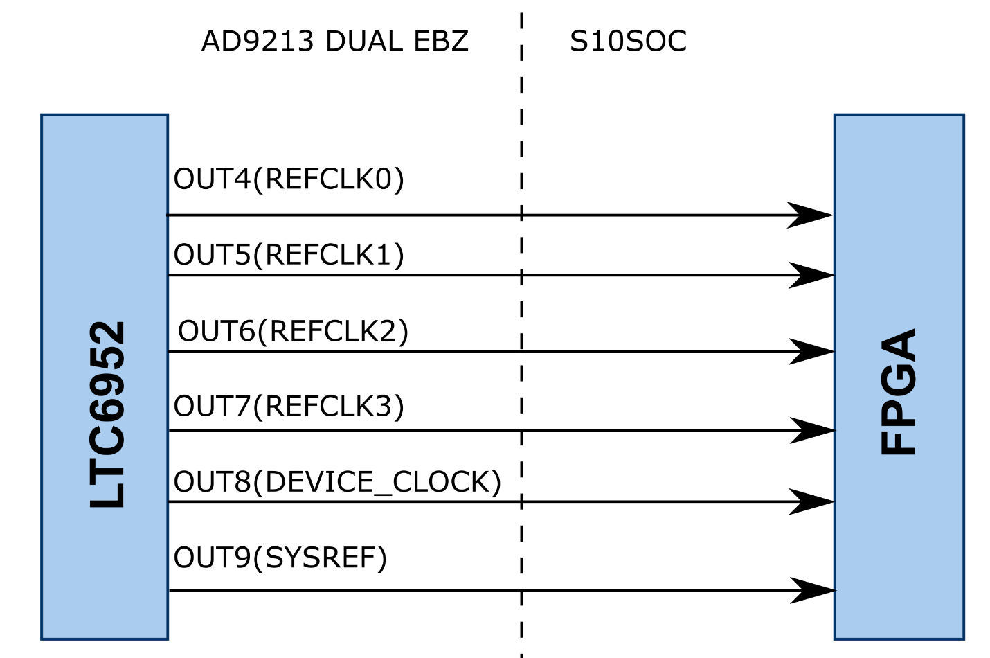
Both physical layer transceiver modules receive two reference clocks from LTC6952 OUT4-7 outputs. The global clock (LaneRate/40) it is received directly from the OUT8 output and SYSREF is received from OUT9 output of the LTC6952.
More Information
Support
Analog Devices will provide limited online support for anyone using the core with Analog Devices components (ADC, DAC, Video, Audio, etc) via the EngineerZone.
resources/eval/user-guides/ad9213_dual_ebz/ad9213_dual_ebz_hdl.1648453052.txt.gz · Last modified: 28 Mar 2022 09:37 by Adrian Costina