


The most recent version of this page is a draft. This version (02 Jun 2023 04:05) was approved by Chelsea Faye Aure.The Previously approved version (31 May 2023 15:20) is available.
This version (02 Jun 2023 04:05) was approved by Chelsea Faye Aure.The Previously approved version (31 May 2023 15:20) is available.This is an old revision of the document!
Table of Contents
ADSKPMB10-EV-FMCZ User Guide
Features
- Fully Isolated PMOD-to-FMC interposer board
- Software programmable bipolar input ranges (±1.1 V to ±11.0 V)
► Allows single-ended and differential signals - GΩ input impedance allows direct interface with sensors
- On-board 5 V reference and buffer
- Complete power management solution
- SPI-/QSPI-/MICROWIRE-/DSP-compatible serial interface
- PC software for control and data analysis of time and frequency domain
Evaluation Kit Contents
- Fully Isolated PMOD-to-FMC Board
- PGIA+ADAQ4003 Data Acquisition Board
Equipment Needed
- System Demonstration Platform Board: SDP-H1 (EVAL-SDP-CH1Z)
- DC/AC signal source (Audio Precision or similar high performance signal source)
- SMA cables
- XLR-SMA interposer board
- Standard USB A to USB mini-B
- PC running Windows 7, 8, or 10 with USB 2.0 port
Software Required
- ADSKPMB10-EV-FMCZ Evaluation Software
General Description
The ADSKPMB10-EV-FMCZ signal chain kit (Figure 1) is part of the Precision Medium Bandwidth evaluation board plus series. It is a two-board solution consist of a Precision Medium Bandwidth Data Acquisition Solution on a PMOD form factor and a Fully Isolated PMOD-to-FMC interposer board.
The Precision Medium Bandwidth Data Acquisition Solution features a discrete programmable gain instrumentation amplifier (PGIA) that was built using a 30V, High Speed, Low Noise, Low Bias Current, JFET Operational Amplifier, the ADA4627-1, a Precision Quad Matched Resistor Network, the LT5400, a Low Capacitance, 4-Channel, ±15 V/+12 V iCMOS™ Multiplexer, the ADG1209 and the internal Fully Differential Amplifier (FDA) ADC driver of the ADAQ4003. The PGIA in thru front-end offers high input impedance that allows direct interface with a variety of sensors. A programmable gain is often needed to adapt the circuit to different input signal amplitudes—unipolar or bipolar and single-ended or differential with varying common-mode voltages. The PGIA works with the ADAQ4003, an 18-Bit, 2 MSPS, µModule® Data Acquisition Solution.
The Fully Isolated PMOD-to-FMC interposer board was designed using a Low Noise, 1A, 1MHz Push-Pull DC/DC Driver with Duty Cycle Control, the LT3999, a Robust 3.0kVrms Digital Isolators w/ Fail-Safe for the SPI lines and PGIA gain control pins, the ADuM152N and the ADuM120N, and a Low noise and ultra-low noise LDO regulators the ADP7105 and the ADP150N respectively.
 Figure 1. Signal Chain Kit
Getting Started
The following section contains the installation instructions for the ADSKPMB10-EV-FMCZ Evaluation Software and the drivers for the SDP hardware required for operation of the software. The evaluation software provides a graphical user interface (GUI) for quick evaluation of the ADSKPMB10-EV-FMCZ.
Software Installation Procedures
Download the evaluation board software from the ADSKPMB10-EV-FMCZ evaluation board page on the Analog Devices website. To install the software, take the following steps:
- Run the ADSKPMB10-EV-FMCZ Evaluation Software installation
- Run the SDP-H1 board drivers installation
Warning
To ensure that the evaluation system is correctly recognized when it is connected to the PC, install the evaluation software and drivers first before connecting the ADSKPMB10-EV-FMCZ and SDP-H1 board to the USB port of the PC.
Installing the ADSKPMB10-EV-FMCZ Evaluation Software
 Figure 2. Unzip the ADSKPMB10-EV-FMCZ Evaluation Software Installer
 Figure 3. ADSKPMB10-EV-FMCZ Evaluation Software Installation — Installation Begins
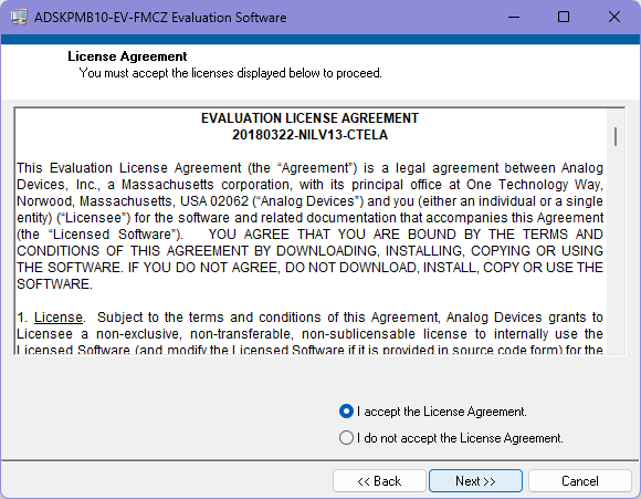 Figure 4. ADSKPMB10-EV-FMCZ Evaluation Software Installation — Selecting the Location for Software Installation (Default Location Shown)
 Figure 5. ADSKPMB10-EV-FMCZ Evaluation Software Installation — Accept the License Agreement
 Figure 6. ADSKPMB10-EV-FMCZ Evaluation Software Installation — Installation Summary
 Figure 7. ADSKPMB10-EV-FMCZ Evaluation Software Installation — Installation Progress
 Figure 8. ADSKPMB10-EV-FMCZ Evaluation Software Installation — Installation Complete
Installing the SDP-H1 Board Drivers
 Figure 9. SDP-H1 Drivers Setup — Beginning the Drivers Installation
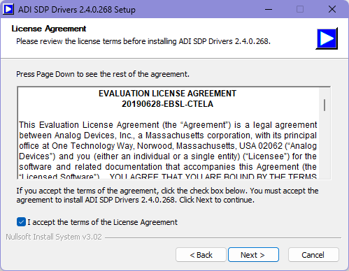
 Figure 10. SDP-H1 Drivers Setup — License Agreement
 Figure 11. SDP-H1 Drivers Setup — Pre-Requisites Checkbox
 Figure 12. SDP-H1 Drivers Setup — Selecting the Location for Drivers Installation
 Figure 13. SDP-H1 Drivers Setup — Beginning the Installation
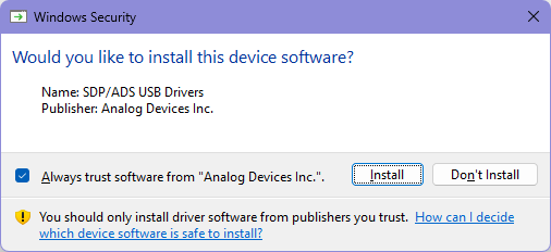 Figure 14. SDP-H1 Drivers Setup — Granting Permission to Install Drivers
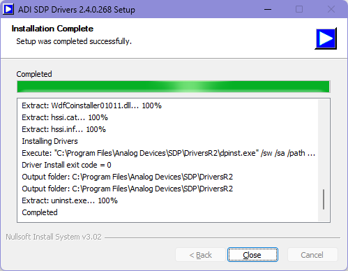 Figure 15. SDP-H1 Drivers Setup — Completing the Drivers Setup Wizard
 Figure 16. SDP-H1 Drivers Setup — Restarting the PC
Hardware Connection
The ADSKPMB10-EV-FMCZ connects to the SDP-H1. The SDP-H1 board serves as the communication link between the PC and ADSKPMB10-EV-FMCZ. Figure 17 shows the connections between the ADSKPMB10-EV-FMCZ and the SDP-H1 board.
Connecting ADSKPMB10-EV-FMCZ and SDP-H1 to a PC
After installing the ACE software, follow these steps to set up the ADSKPMB10-EV-FMCZ and SDP-H1, as shown in Figure 18.
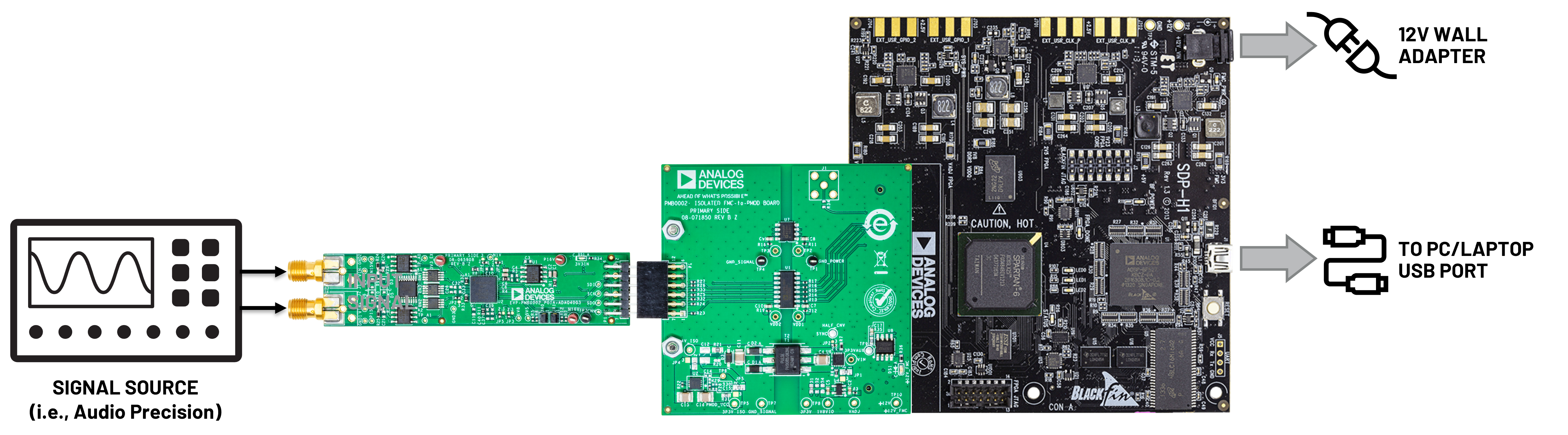
Figure 17. Signal Chain Kit Connection
- Ensure all configuration links are in the appropriate positions, as detailed in Table 1.
- Connect the ADSKPMB10-EV-FMCZ securely to the 160-way connector on the SDP-H1. The ADSKPMB10-EV-FMCZ does not require an external power supply adapter.
- Connect the SDP-H1 to the PC through the USB cable and power it up with the 12 V wall adapter included in the SDP-H1 kit.
Verifying the Board Connection
After completing Software Installation Procedures and Evaluation Board Setup, follow these steps to verify the board connection:
- Run the Found New Hardware Wizard after the SDP-H1 system demonstration platform board is plugged into the PC. If using Windows XP, search for the SDP-H1 drivers. Automatically search for the drivers of the SDP-H1 system demonstration platform board, if prompted by the operating system.
- Check the evaluation board is connecting to the PC correctly using the Device Manager of the PC. Access the Device Manager as follows:
- Right click My Computer and then click Manage.
- A dialog box appears seeking permission to allow the program to make changes to the computer. Click Yes.
- The Computer Management window appears. Click Device Manager from the list of System Tools (see Figure 18)
- If the SDP-H1 system demonstration platform board appears under ADI Development Tools, the driver software is installed and the evaluation board is connecting to the PC correctly.
 Figure 18. Checking that the ADSKPMB10-EV-FMCZ is connected to the PC correctly
Disconnecting ADSKPMB10-EV-FMCZ
Disconnect the ADSKPMB10-EV-FMCZ from the SDP-H1 by either:
- Turning off the power from the SDP-H1 by unplugging the 12 V wall wart adapter.
- Pressing the reset tact switch located alongside the mini-USB port on the SDP-H1.
Hardware Description and Performance

Figure 19. Simplified Evaluation Board Block Diagram
Figure 19 shows the simplified block diagram of the ADSKPMB10-EV-FMCZ, which is composed of the two boards: the PMOD-to-FMC interposer board and the PGIA + ADAQ4003 Data Acquisition Board.
The PMOD-to-FMC interposer board consists of the digital isolators, ADuM152N (U1) and ADuM120N (U7), the DC/DC regulator LT3999 (U6), and lastly, the LDO regulators, ADP7105 (U2) and ADP150N (U4).
The PGIA + ADAQ4003 Data Acquisition Board consists of the ADAQ4003 µModule (U2), a 5.0 V reference (U1, ADR4550), the analog front-end circuitry — with the discrete PGIA (A1 and A2, ADA4627-1), the ADG1209 (U5) multiplexer, the precision quad matched resistor network (RN1, RN2, and RN3, LT5400) — and lastly, the on-board power supplies to derive the necessary supply rails, namely, the (U3, ADP5070), (U2, LT3032), and (U6, LT3023).
Power Supplies
Fully Isolated PMOD-to-FMC Interposer Board
The Fully Isolated PMOD-to-FMC interposer board was designed using a Low Noise, 1A, 1MHz Push-Pull DC/DC Driver with Duty Cycle Control, the LT3999, a Robust 3.0 kVrms Digital Isolators w/ Fail-Safe for the SPI lines and PGIA gain control pins, the ADuM152N and the ADuM120N, and a Low noise and ultra low noise LDO regulators the ADP7105 and the ADP150N respectively.
The interposer board was designed to cater multiple VIO voltage levels. The user has 3 options on the FMC VIO side and by default, the VIO is connected or set by FMC's VADJ pin. 3.3 V and 1.8 V is also available in case other VIO voltage level is needed as shown in Figure 20 below.
 Figure 20. FMC side VIO Options
On the PMOD side, the user has an option to connect the VCC pin of the PMOD Data Acquisition device directly to LT3999's push-pull transformer output or to provide a regulated 3.3 V output using the ADP7105. By default, the PMOD VCC is powered directly from the LT3999's push-pull transformer output as shown in Figure 21 below.
 Figure 21. PMOD VCC Options
PGIA + ADAQ4003 Data Acquisition Board
The SDP-H1 supplies 3.3 V to power the rails for the different components on the PGIA + ADAQ4003 Data Acquisition Board. The ADAQ4003 µModule use four power supply pins: the ADC driver positive supply (VS+), the ADC driver negative supply (VS−), the core ADC supply (VDD), and the digital input and output interface supply (VIO). The VIO pin allows the direct interface with any logic between 1.8 V and 5.5 V. A combination of the ADP5070 (dual, high-performance dc-to-dc switching regulator), the LT3032 (dual, low noise, positive and negative low dropout voltage linear regulator), and the LT3023 (dual, micropower, low noise, low dropout regulator) can generate independently regulated positive and negative rails for all four power supply pins, including ±15 V rails for any additional signal conditioning.
Table 1. Default Power Supplies

Each supply is decoupled at the PGIA + ADAQ4003 Data Acquisition Board entrance and device connection. A single, on-board ground plane minimizes the effect of the high frequency noise interference.
In addition, the PGIA + ADAQ4003 Data Acquisition Board can be powered from a benchtop power supply of ±16 V. The +16 V, −16 V, and GND test points are available on board to support this function. When bench power is used, the on-board power supplies are no longer required, and the link between the output pin of the ADP5070 must be removed, that is, uninstall R65 and R66.
Take the following steps to set up the PGIA + ADAQ4003 Data Acquisition Board when using a benchtop power supply of ±16 V:
- Connect the PGIA + ADAQ4003 Data Acquisition Board to the Isolated PMOD-to-FMC interposer board at the P1 header (see Figure 17).
- Connect the Isolated PMOD-to-FMC interposer board to the SDP-H1 via the 160-pin FMC connector.
- Connect the USB and a 12 V power adapter to the SDP-H1. Ensure that the software and drivers are installed.
- Connect the +16 V and −16 V bench supplies to the +16 V and −16 V test points on the PGIA + ADAQ4003 Data Acquisition Board. Connect also the bench supply ground to the GND test point (see Figure 22).
- Power up the benchtop supply. The +16 V supply rail draws approximately 25 mA, and the −16 V supply rail draws approximately 20 mA.
 Figure 22. External Supply Optional Connections
The evaluation kit is now ready to use. Note that by default, the PGIA + ADAQ4003 Data Acquisition Board are set up to accept a differential input with a 22 V range.
SDP-H1 Controller Board
The ADSKPMB10-EV-FMCZ evaluation board uses the serial peripheral interface (SPI) and is connected to the high speed controller board for the system demonstration platform (SDP-H1) controller board. The SDP-H1 board requires power from a 12 V wall adapter. The SDP-H1 has the Xilinx® Spartan 6 and ADSP-BF527 processor with connectivity to the PC through a USB 2.0 high speed port. The controller boards configure and capture data on the daughter boards from the PC through a USB.
The SDP-H1 has an FMC low pin count (LPC) connector with full differential LVDS and singled-ended LVCMOS support. It also features the 160-pin connector, found on the SDP-B, which exposes the Blackfin® processor peripherals. This connector provides a configurable serial, parallel I²C and SPI, and general-purpose input/output (GPIO) communication lines to the attached daughter board for the functional description of the on-board power supplies.
Analog Inputs
The analog input signals of the board are the Subminiature Version A (SMA) connectors, J3 and J4, by default. Similarly, an option for the Subminiature Version B (SMB) connectors, J1 and J2 are also available. These analog inputs are fed to the dedicated amplifier circuitry, ADA4627-1 (A1 and A2), and are set as unity-gain buffers at the factory.
The analog inputs are fully differential by default, with both inputs floating with high impedance. Thus, ensure the signal source is properly biased to a common-mode voltage. See Table 2 for input range configuration and control.
Measure the true dynamic range of the board by connecting the two inputs to the board’s ground reference by using SMA terminators (see Figure 23).
 Figure 23. Short the inputs to ground using SMA terminators to measure the Signal Chain Dynamic Range
For dynamic performance, a fast Fourier transform (FFT) test can be performed by applying a low distortion AC source. For low frequency testing, the audio precision source, such as the APx500 series, can be used directly with the evaluation boards. Different precision sources can be used with additional filtering.
Hardware Link Options
Set the multiple link options correctly for the appropriate operating setup before applying the power and signal to the ADSKPMB10-EV-FMCZ. Table 1 shows the default link positions for the ADSKPMB10-EV-FMCZ.
Table 1. Jumper Details with Factory Default Setting

Precision Medium Bandwidth Data Acquisition Solution
This Data Acquisition Solution has 4 gain options, as shown in Table 2. The gain of the signal chain can be controlled by changing the logic levels of the ADG1209 A0 and A1 pins. This can be done through the software or by adjusting the jumpers JA0 and JA1.
Table 2. System Gain and Input Range 
Figure 24 shows the Dynamic Range vs. Gain Performance of the data acquisition solution.

Figure 24. Dynamic Range vs. Gain
Figure 25 shows the Signal-to-Noise Ratio (SNR) vs. Frequency vs. Gain Performance of the data acquisition solution.

Figure 25. SNR vs. Frequency vs. Gain
Figure 26 shows the Total Harmonic Distortion (THD) vs. Frequency vs. Gain Performance of the data acquisition solution.

Figure 26. THD vs. Frequency vs. Gain
Software GUI Setup
Launching the Software
After installing the ADSKPMB10-EV-FMCZ Evaluation Software Installer (see the Software Installation Procedures section), run the software with either of the following methods:
- Navigate to the destination folder of the ADSKPMB10-EV-FMCZ Evaluation Software Installer selected during the installation procedure and run the ADSKPMB10-EV-FMCZ.exe file.
- Click Start > All Programs > Analog Devices > ADSKPMB10-EV-FMCZ.
 Figure 27. Launching the Software
Establishing Hardware Connection
After the ADSKPMB10-EV-FMCZ Evaluation Software initializes, the software front panel appears, and the software automatically connects to any ADSKPMB10-EV-FMCZ evaluation board connected to the PC. The detected evaluation board is displayed in the Eval Board Connected indicator on the front panel (see Label 15 in Figure 29).
If the software does not detect a valid ADSKPMB10-EV-FMCZ evaluation board, a connectivity error dialog box appears (see Figure 28). Clicking the Rescan button instructs the software to try to detect the hardware again. Clicking the Cancel button causes the software to boot in offline mode.
 Figure 28. Connectivity Error Dialog Box
Navigating the Evaluation Software
 Figure 29. ADSKPMB10-EV-FMCZ Evaluation Software Front Panel (Configure Tab View)
Front Panel Overview
The ADSKPMB10-EV-FMCZ Evaluation Software front panel is shown in Figure 29. The following sections describe the various software controls accessible on the front panel.
File Menu
The File menu (Label 1 in Figure 29) provides the following options:
- Save Captured Data (Ctrl + S): saves the current session in a .csv file. The user is prompted to either choose or enter the path of the file in the Save As dialog box. This saved file can be loaded by the software at a future time to display previously captured data.
- Load Captured Data (Ctrl + O): opens the Load File dialog box and the user is prompted to load the previously saved evaluation software session files (.csv). Don't forget to click Single Capture to view the saved session files.
- Take Screenshot: saves the current front panel display as an image file (.jpg). The user is prompted to either choose or enter the path of the file in a Save As dialog box.
- Print Screenshot: sends a screenshot of the current front panel display directly to the default printer identified by the operating system for printing.
- Exit: closes the front panel and exits the software.
Edit Menu
The Edit menu (Label 1 in Figure 29) provides the following options:
- Reinitialize Default Values: resets a subset of the evaluation software front panel controls to the default state.
Help Menu
The Help menu (Label 1 in Figure 29) provides the following options:
- ADAQ4003 Evaluation Hardware Info: opens the ADAQ4003 product page in the default browser of the PC.
- Context Help (Ctrl + H): displays a context help dialog box, which displays information about the various software controls when the mouse hovers over them.
- About (Ctrl + A): displays version and copyright information of the evaluation software in a dialog box.
Display Tabs
The following five tabs are located at the top of the front panel (Label 2 in Figure 29): Configure, Waveform, Histogram, FFT, and Summary. These tabs select various front panel views.
Single Capture Button
Click Single Capture (Label 3 in Figure 29) to perform a single set of conversions. The number of conversions performed is set with the Samples dropdown list, which is located to the left of the Single Capture control.
Continuous Capture Button
Click Continuous Capture (Label 4 in Figure 29) to perform repeated sets of conversions. The number of conversions performed per set is set with the Samples dropdown list.
Samples Dropdown List
The Samples dropdown list (Label 5 in Figure 29) sets the number of conversions that are performed when Single Capture or Continuous Capture is clicked.
Status Bar
The status bar (Label 6 in Figure 29) displays information about the current process being completed by the evaluation software. The Status Bar includes a Busy indicator, which displays if the software is busy performing a task such as performing conversions, analyzing results, and so on.
Configure Tab View
Figure 29 shows the Configure tab view. The Configure tab provides controls for configuring the connected device and software settings. The Configure tab view contains the following controls and indicators:
- Eval Board Connected (Label 6 in Figure 29): indicates that the evaluation board is connected to the software.
- Oversampling Ratio (Label 7 in Figure 29): sets the oversampling ratio applied to the captured data. After this control is set to any value other than None, the software sums up the consecutive conversion results together to increase effective resolution. The number of conversions summed together is set by the Oversampling Ratio control.
- Throughput (kSPS) (Label 8 in Figure 29): sets the throughput of the connected device. The maximum value of this control is automatically set to reflect the maximum achievable throughput of the connected device, given the state of the Status Bits and Turbo Mode controls. See the relevant ADAQ4003 device data sheet for more information on maximum achievable throughput.
- Gain Control (Label 8 in Figure 29): sets the PGIA Front-end Gain of the device. The user can choose from 1, 2, 5, or 10.
- Voltage Reference (VREF) (Label 10 in Figure 29): sets the VREF used in data analysis such as when calculating LSB Size (see Label 2 in Figure 30), or measured voltage in the waveform graph (see the Waveform Tab View section. This control must be set to match the VREF used on the connected evaluation board.
- Device Config Settings (Label 11 in Figure 29): configures the connected device user configuration register settings. See the relevant ADAQ4003 device data sheet for a detailed description of the user configuration register and the device features.
- Status Bits: enables or disables the status bits for the connected device.
- Span Compression: enables or disables span compression for the connected device.
- High-Z Mode: enables or disables high-Z mode.
- Turbo Mode: enables or disables turbo mode for the connected device.
- Read Register (Label 12 in Figure 29): reads the device user register. When Read Register is clicked, the contents of the connected device register are read to update the Device Config Settings items accordingly.
- Device configuration settings display (Label 13 in Figure 29): displays the status of the user register when Read Register is clicked. Each of the following indicators displays the state of the corresponding settings:
- Status Bits, Span Compression, High-Z Mode, and Turbo Mode status indicators indicate whether the corresponding device are reported as enabled or disabled in the user configuration register.
- Overvoltage Clamp Flag: indicates the status of the OV clamp flag in the user configuration register of the connected device. When this indicator is red, the OV flag is low, indicating the presence of an overvoltage event.
- Status Bits Indicators (Label 14 in Figure 29): displays the configuration settings of the device as indicated by the status bits. The status bits are enabled with the Status Bits control in the Device Config Settings pane (Label 11 in Figure 29). The Status Bits Indicators are only updated after conversions are performed with the Single Capture or Continuous Capture controls when the status bits are enabled on the connected device. The status bit functionality is described in the relevant ADAQ4003 device data sheet.
- The Span Compression, High-Z Mode, and Turbo Mode status indicators indicate whether features of the corresponding device are reported as enabled or disabled by the status bits.
- Overvoltage Clamp Flag: displays whether the OV clamp flag in the status bits indicated an overvoltage event in any of the conversions in the most recently displayed results. When this indicator is red, the OV flag is low, indicating the presence of an overvoltage event. See the ADAQ4003 datasheet for more details on the OV clamp flag.
Waveform Tab View
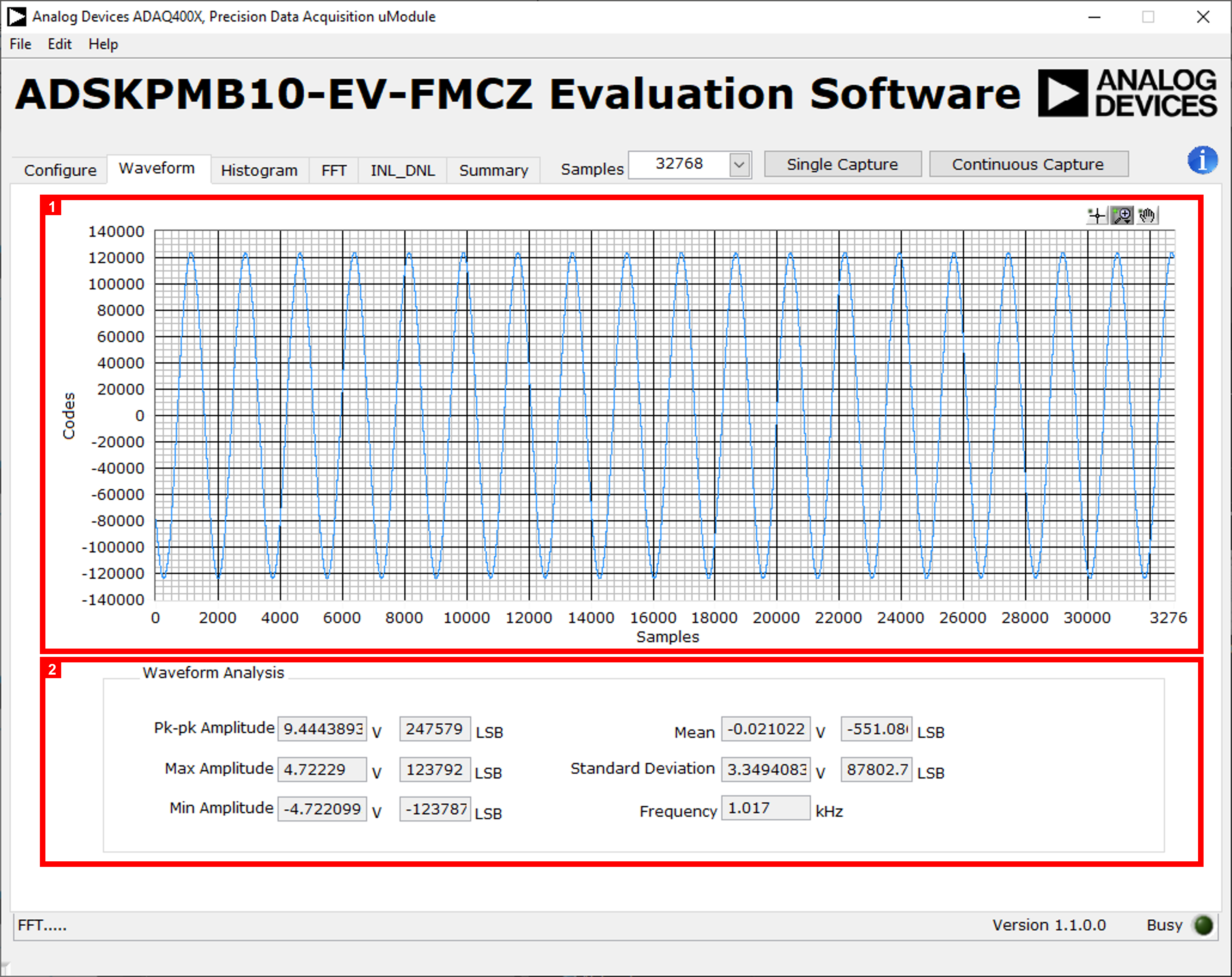 Figure 30. Waveform Tab View
Figure 30 shows the Waveform tab view. The Waveform tab view shows the time domain representation of the conversion results from the connected device, as well as several analysis items. The Waveform tab view contains the following controls and indicators:
- Waveform graph (Label 1 in Figure 30): displays the time domain plot of the most recently captured or loaded conversion results. The scale and range of the waveform graph can be set in the Waveform Analysis box by double clicking on the Minimum Value and Maximum Value fields and entering the desired values. The waveform graph also includes viewing tools that are described in Graph Viewing Controls section.
- Waveform Analysis (Label 2 in Figure 30): shows the following analysis items for the currently displayed data.
- Pk-Pk Amplitude: displays the peak-to-peak amplitude of the captured data (the difference between the Max Value and the Min Value).
- Max Amplitude: displays the maximum value measured in the captured data.
- Min Amplitude: displays the minimum value measured in the captured data.
- Mean: displays the arithmetic mean of the captured data.
- Standard Deviation: displays the standard deviation of the captured data.
- Frequency: displays the frequency of the captured data.
Histogram Tab View
 Figure 31. Histogram Tab View
Figure 31 shows the Histogram tab view. The Histogram tab is useful for performing statistical analysis of the device conversion results, especially when measuring DC signals. The histogram graph shows the distribution of the conversion results as well as various statistical analysis items. The Histogram tab contains the following controls and indicators:
- Histogram graph (Label 1 in Figure 31): displays histogram of the most recently captured or loaded conversion results. The scale and range of the histogram graph can be set by double-clicking on the minimum and maximum axis values and entering the desired values. The histogram graph also includes viewing tools, described in Table 5.
- Histogram Analysis (Label 2 in Figure 31): shows the following analysis items for the currently displayed data.
- Max Value: displays the maximum value measured in the captured data.
- Min Value: displays the minimum value measured in the captured data.
- DC Offset/Mean: displays the arithmetic mean of the captured data.
- Transition Noise: displays the transition noise of the captured data.
- Pk-Pk Amplitude: displays the peak-to-peak amplitude of the captured data (the difference between the Maximum Value and the Minimum Value).
- RMS: displays the measured RMS voltage.
- LSB: displays the effective size (in μV) of each LSB given the resolution of the connected device, and the Voltage Reference (VREF) and Oversampling Ratio values selected in the Configure tab.
- Histogram Width: displays the size of the bins in the histogram graph x-axis.
FFT Tab View
 Figure 32. FFT Tab View
Figure 32 shows the FFT tab view. The FFT tab displays the calculated FFT representation of the conversions results from the connected device and common AC performance metrics. The FFT tab contains the following controls and indicators:
- FFT graph (Label 1 in Figure 32): displays an FFT of the most recently captured or loaded conversion results. Set the scale and range of the FFT graph by double clicking on the minimum and maximum values along the x-axis and y-axis and entering the desired values. The FFT graph also includes viewing tools that described in Table 5.
- FFT Analysis (Label 2 in Figure 32): displays common ac performance metrics of the captured data. Results are calculated from the FFT spectrum, typically ignoring the first six frequency bins.
- Max Amplitude: displays the maximum value measured in the captured data.
- Min Amplitude: displays the minimum value measured in the captured data.
- Pk-Pk Amplitude: displays the peak-to-peak amplitude of the captured data (the difference between the Maximum Value and the Minimum Value).
- DC: displays the DC value of the captured data.
- Fund. Frequency: displays the frequency identified as fundamental, the frequency bin with the largest signal.
- Fund. Amplitude: displays amplitude of the fundamental frequency, the frequency bin with the largest signal.
- Dynamic Range: displays the calculated dynamic range.
- RMS: displays the measured RMS voltage.
- SNR: displays the calculated signal-to-noise ratio (SNR).
- THD: displays calculated total harmonic distortion (THD), up to the fifth harmonic.
- SINAD: displays the calculated single-to-noise and distortion ratio (SINAD).
- Noise Floor: displays the average amplitude of noise frequency bins, more specifically, bins not identified as fundamental or harmonic.
- Bin Width: displays the size of the frequency bins in the FFT graph x-axis. The bin width is a function of both the Throughput (kSPS) control (Label 8 in Figure 29) and the number of samples in the captured data.
- SFDR: displays the calculated spurious-free dynamic range (SFDR).
- Show Harmonic Content: contains Frequency and Amplitude information for the fundamental and harmonic tones identified in the FFT. These displays are only visible when toggled by the Show Harmonic Content control and are not displayed in Figure 32.
- Frequency: frequency bins identified as fundamental and harmonic.
- Amplitude: amplitude of the fundamental and harmonic frequencies.
Summary Tab View
 Figure 33. Summary Tab View
Figure 33 shows the Summary tab view. The Summary tab simultaneously displays the waveform, histogram, and FFT graphs and analysis for the device conversion results on the screen. The Summary tab contains the following controls and indicators:
- Waveform graph (Label 1 in Figure 33): displays the time domain plot of the most recently captured or loaded conversion results. The scale and range of the waveform graph can be set by double-clicking on the minimum and maximum axis values along the x-axis and y-axis and entering the desired values. The waveform graph also includes viewing tools that are described in Graph Viewing Controls section.
- Histogram graph (Label 2 in Figure 33): displays the histogram of the most recently captured or loaded conversion results. The scale and range of the histogram graph can be set by double-clicking on the minimum and maximum values along the x-axis and y-axis and entering the desired values. The histogram graph also includes viewing tools that are described in Graph Viewing Controls section.
- FFT graph (Label 3 in Figure 33): displays an FFT of the most recently captured or loaded conversion results. The scale and range of the FFT graph can be set by double clicking on the minimum and maximum axis values and entering the desired values. The FFT graph also includes viewing tools that are described in Graph Viewing Controls section.
- Analysis Summary (Label 4 in Figure 33): shows the following analysis items for the currently displayed data.
- Pk-Pk Amp: displays the peak-to-peak amplitude of the captured data.
- DC Offset/Mean: displays the arithmetic mean of the captured data.
- Transition Noise: displays the transition noise of the captured data.
- Fund. Freq.: displays frequency identified as the fundamental (the frequency bin with the largest signal).
- Fund. Amp.: displays the amplitude of the Fund. Freq.
- RMS: displays the measured RMS voltage of the captured data.
- Dynamic Range: displays the calculated dynamic range of the captured data.
- SNR: displays the calculated SNR of the captured data.
- THD: displays the calculated THD of the captured data (up to the fifth harmonic).
- SINAD: displays the calculated SINAD of the captured data.
- LSB: displays the effective size (in μV) of each LSB. The LSB size is a function of the resolution of the connected device, the Reference Voltage (VREF), and Oversampling Ratio values selected in the Configure tab.
- SFDR: displays the calculated SFDR of the captured data.
Graph Viewing Controls
The tools described below allow users to control the different chart displays within any of the chart panels in the graphical user interface (GUI) tabs.
| Symbol | Description |
|---|---|
 | This tool controls the cursor, if present. |
 | This tool zooms in and out of the data on the graph. |
 | This tool is used for panning. |
Saving and Loading Sessions
The ADSKPMB10-EV-FMCZ Evaluation Software allows users to save and load data to quickly recall previous results. Clicking File > Save Captured Data or using the shortcut Ctrl + S saves the capture data and relevant sampling parameters for the currently displayed device in a .csv file. These saved files can be loaded at a later time by clicking File > Load Captured Data or using the shortcut Ctrl + O. Upon loading these .csv files, the evaluation software displays the data in the Waveform, Histogram, FFT, and Summary tabs.
The evaluation software also allows the user to export the raw data of any of the graphs into a generic text file by right clicking them and selecting Export > Export Data to Excel, as shown in Figure 34. The exported data can be used for additional postprocessing, but the generated text file cannot be loaded back into the ADSKPMB10-EV-FMCZ Evaluation Software.
 Figure 34. Export Raw Data
Schematic, PCB Layout, Bill of Materials
ADSKPMB10-EV-FMCZ Design & Integration Files
- Schematics
- PCB Layout
- Bill of Materials
- Allegro Project
Troubleshooting
Software
To troubleshoot the software, take the following steps:
- Always install the software before connecting the hardware to the PC.
- Make sure to completely finish the installation (the software is a two-part installation, the evaluation software and the SDP-H1 drivers). A restart is recommended after installation is finished.
- When the user initially plugs in the SDP-H1 via the provided USB cable, allow the Found New Hardware Wizard to run, which can take several seconds. Allow this to happen first before starting the software.
- If the ADSKPMB10-EV-FMCZ or SDP-H1 board are connected to the PC via the USB port, but are not detected by the software, ensure that the board is being recognized in the Device Manager, as shown in Figure 18.
- If connected to a slower USB port where the SDP-H1 cannot read as quickly as it needs to, a timeout error can result. In this case, it is advised not to read continuously, or alternatively, to lower the number of samples taken.
Hardware
To troubleshoot the hardware, take the following steps:
- If the software does not read back any data, do the following:
- Check that the power is applied within the power ranges described in the Power Supplies section.
- Using a voltmeter, measure the voltage present at each of the test points: P15V, N15V, N1V, 1V8, and 5V5. Note that the LED1 on the SDP-H1 must be lit.
- Launch the software and read the data. If nothing happens, exit the software.
- Power down the board and relaunch the software.
- If no data is read back, confirm that the evaluation board is connected to the SDP-H1, and that the SDP-H1 is being recognized in the Device Manager, as shown in Figure 18.
- When the user is working with the software in standalone/offline mode (no hardware connected) and later chooses to connect hardware, close and relaunch the software.
Additional Information and Useful Links
Software Projects and Platforms
- N/A
Registration
Receive software update notifications, documentation updates, view the latest videos, and more when you register your hardware. Register to receive all these great benefits and more!
End of Document
/srv/wiki.analog.com/data/pages/resources/eval/user-guide/adskpmb10-ev-fmcz.txt · Last modified: 05 Mar 2024 04:32 by Chelsea Faye Aure