


This version (09 Feb 2021 18:58) was approved by Istvan Csomortani.The Previously approved version (30 Jan 2012 12:25) is available.
Table of Contents
SDP-B Hardware Description
This describes the hardware design of the EVAL-SDP-CB1Z board.
This board is full of niubility! By using it, you can create a colorful world! After you entering this vivid world,you will feel of rebirth,and then you will shout “Hello World!”.
LEDs
There are two LEDs located on the SDP-B board. Refer to Figure HWD1.

Figure HWD1: SDP-B Board LEDs
LED 1
The orange LED is an LED to be used as a diagnostic tool for evaluation application developers.
POWER LED (LED2)
The green power LED indicates that the SDP-B board is powered. This is not an indication of USB connectivity between the SDP-B and the PC.
Connector Details
The SDP-B board contains two identical Hirose FX8-120P-SV1(91), 120 pin header, connectors. Through these connectors, the peripheral communication interfaces of ADSP-BF527 Blackfin processor are exposed. The exposed peripherals are:
- SPI
- SPORT
- I2C/TWI
- GPIO
- Asynchronous Parallel
- PPI
- UART
- Timers
Also, included on the connector specification are input and output power pins, ground pins, and pins reserved for future use.
For further details on the peripheral interfaces, including timing diagrams, see the ADSP-BF52x Blackfin Processor Hardware Reference
Connector C exposes the entire Blackfin memory space but is not used as part of the SDP platform.
Connector Pin Assignments
The connector pin assignments for Connector A and Connector B have been defined independently of the any internal pin sharing that occurs on the Blackfin processor. The below table lists the connector pins and identifies the functionality assigned to each connector pin for Connector A and Connector B on the SDP-B board.
120 Pin Connector Pin Assignments
| Pin No. | Pin Name | Description |
|---|---|---|
| 1 | VIN | Power to SDP-B board. Requires 200mA @ 4 – 7 Volts. |
| 2 | NC | No Connect. Leave this pin unconnected. Do not ground. |
| 3 | GND | Connect to ground plane of board. |
| 4 | GND | Connect to ground plane of board. |
| 5 | USB_VBUS | Connected directly to the USB +5v Supply. |
| 6 | GND | Connect to ground plane of board. |
| 7 | PAR_D23 | Parallel Data Bus Bit 23.(No connect.) 1 |
| 8 | PAR_D21 | Parallel Data Bus Bit 21.(No connect.) 1 |
| 9 | PAR_D19 | Parallel Data Bus Bit 19.(No connect.) 1 |
| 10 | PAR_D17 | Parallel Data Bus Bit 17.(No connect.) 1 |
| 11 | GND | Connect to ground plane of board. |
| 12 | PAR_D14 | Parallel Data Bus Bit 14. |
| 13 | PAR_D13 | Parallel Data Bus Bit 13. |
| 14 | PAR_D11 | Parallel Data Bus Bit 11. |
| 15 | PAR_D9 | Parallel Data Bus Bit 9. |
| 16 | PAR_D7 | Parallel Data Bus Bit 7. |
| 17 | GND | Connect to ground plane of board. |
| 18 | PAR_D5 | Parallel Data Bus Bit 5. |
| 19 | PAR_D3 | Parallel Data Bus Bit 3. |
| 20 | PAR_D1 | Parallel Data Bus Bit 1. |
| 21 | PAR_RD | Low Enable. Asynchronous Parallel Read Strobe. |
| 22 | PAR_CS | Low Enable. Asynchronous Parallel Chip Select. |
| 23 | GND | Connect to ground plane of board. |
| 24 | PAR_A3 | Parallel Address Bus Bit 3. |
| 25 | PAR_A1 | Parallel Address Bus Bit 1. |
| 26 | PAR_FS3 | Synchronous (PPI) Parallel Frame Sync 3. |
| 27 | PAR_FS1 | Synchronous (PPI) Parallel Frame Sync 1. |
| 28 | GND | Connect to ground plane of board. |
| 29 | SPORT_TDV0 | SPI Data Receive 3. (No connect.) 1 |
| 30 | SPORT_TDV1 | SPI Data Receive 2. (No connect.) 1 |
| 31 | SPORT_DR1 | SPORT Data Receive 1. Secondary SPORT Data into processor. |
| 32 | SPORT_DT1 | SPORT Data Transmit 1. Secondary SPORT Data from processor. |
| 33 | SPI_D2 | SPORT Data Transmit 2.(No connect.) 1 |
| 34 | SPI_D3 | SPORT Data Transmit 3.(No connect.) 1 |
| 35 | SERIAL_INT | Serial Interrupt. Used to trigger a non-periodic SPORT event. |
| 36 | GND | Connect to ground plane of board. |
| 37 | SPI_SEL_B | Low enable. SPI Chip Select B. Use this to control a second device on the SPI bus. |
| 38 | SPI_SEL_C | Low enable. SPI Chip Select C. Use this for a third device on the SPI bus. |
| 39 | SPI_SEL1/ SPI_SS | SPI Chip Select 1. 2 Used to connect to SPI Boot Flash if required. Also used as Chip Select when Blackfin processor is operating as SPI Slave. |
| 40 | GND | Connect to ground plane of board. |
| 41 | SDA_1 | I2C Data 1.2 |
| 42 | SCL_1 | I2C Data 1.2 |
| 43 | GPIO0 | General Purpose Input/Output. |
| 44 | GPIO2 | General Purpose Input/Output. |
| 45 | GPIO4 | General Purpose Input/Output. |
| 46 | GND | Connect to ground plane of board. |
| 47 | GPIO6 | General Purpose Input/Output.2 |
| 48 | TMR_A | Timer A flag pin. Use as first Timer if required. |
| 49 | TMR_C | Timer C flag pin.1 (No connect.) |
| 50 | NC | No Connect. Leave this pin unconnected. Do not ground. |
| 51 | NC | No Connect. Leave this pin unconnected. Do not ground. |
| 52 | GND | Connect to ground plane of board. |
| 53 | NC | No Connect. Leave this pin unconnected. Do not ground. |
| 54 | NC | No Connect. Leave this pin unconnected. Do not ground. |
| 55 | NC | No Connect. Leave this pin unconnected. Do not ground. |
| 56 | EEPROM_A0 | EEPROM A0. Connect to A0 Address line of the EEPROM |
| 57 | RESET_OUT | Active low pin to reset controller board. |
| 58 | GND | Connect to ground plane of board. |
| 59 | UART_RX | UART Receive Data.2 |
| 60 | RESET_IN | Active low pin to reset controller board. |
| 61 | BMODE1 | Boot Mode 1. Pull up with 10kΩ resistor to set SDP-B to boot from SPI Flash. Enabled on Connector A only. |
| 62 | UART_TX | UART Receive Data.2 |
| 63 | GND | Connect to ground plane of board. |
| 64 | SLEEP | Active low sleep from processor board. |
| 65 | WAKE | External wake up to processor board. |
| 66 | NC | No Connect. Leave this pin unconnected. Do not ground. |
| 67 | NC | No Connect. Leave this pin unconnected. Do not ground. |
| 68 | NC | No Connect. Leave this pin unconnected. Do not ground. |
| 69 | GND | Connect to ground plane of board. |
| 70 | NC | No Connect. Leave this pin unconnected. Do not ground. |
| 71 | CLKOUT | CLKOUT from processor. |
| 72 | TMR_D | Timer D flag pin.2 |
| 73 | TMR_B | Timer B flag pin. Use as second Timer if required. |
| 74 | GPIO7 | General Purpose Input/Output. |
| 75 | GND | Connect to ground plane of board. |
| 76 | GPIO5 | General Purpose Input/Output. |
| 77 | GPIO3 | General Purpose Input/Output. |
| 78 | GPIO1 | General Purpose Input/Output. |
| 79 | SCL_0 | I2C Clock 0. Daughter Board EEPROM must be connected to this bus. |
| 80 | SDA_0 | I2C Data 0. Daughter Board EEPROM must be connected to this bus. |
| 81 | GND | Connect to ground plane of board. |
| 82 | SPI_CLK | SPI Clock. |
| 83 | SPI_MISO | SPI Master In, Slave Out Data. |
| 84 | SPI_MOSI | SPI Master Out, Slave In Data. |
| 85 | SPI_SEL_A | SPI Chip Select A. Use this to control the first device on the SPI bus. |
| 86 | GND | Connect to ground plane of board. |
| 87 | SPORT_TSCLK | SPORT Transmit Clock. |
| 88 | SPORT_DT0 | SPORT Data Transmit 0. Primary SPORT Data from processor. |
| 89 | SPORT_TFS | SPORT Transmit Frame Sync. |
| 90 | SPORT_RFS | SPORT Receive Frame Sync. |
| 91 | SPORT_DR0 | SPORT Data Receive 0. Primary SPORT Data into processor. |
| 92 | SPORT_RSCLK | SPORT Receive Clock |
| 93 | GND | Connect to ground plane of board. |
| 94 | PAR_CLK | Clock for Synchronous Parallel Interface (PPI). |
| 95 | PAR_FS2 | Synchronous (PPI) Parallel Frame Sync 2. |
| 96 | PAR_A0 | Parallel Address Bus Bit 0. |
| 97 | PAR_A2 | Parallel Address Bus Bit 2. |
| 98 | GND | Connect to ground plane of board. |
| 99 | PAR_INT | Parallel Interrupt. Used to trigger a non-periodic Parallel event. |
| 100 | PAR_WR | Asynchronous Parallel Write Strobe. |
| 101 | PAR_D0 | Parallel Data Bus Bit 0. |
| 102 | PAR_D2 | Parallel Data Bus Bit 2. |
| 103 | PAR_D4 | Parallel Data Bus Bit 4. |
| 104 | GND | Connect to ground plane of board. |
| 105 | PAR_D6 | Parallel Data Bus Bit 6. |
| 106 | PAR_D8 | Parallel Data Bus Bit 8. |
| 107 | PAR_D10 | Parallel Data Bus Bit 10. |
| 108 | PAR_D12 | Parallel Data Bus Bit 12. |
| 109 | GND | Connect to ground plane of board. |
| 110 | PAR_D15 | Parallel Data Bus Bit 15. |
| 111 | PAR_D16 | Parallel Data Bus Bit 16. (No connect.) 1 |
| 112 | PAR_D18 | Parallel Data Bus Bit 18. (No connect.) 1 |
| 113 | PAR_D20 | Parallel Data Bus Bit 20. (No connect.) 1 |
| 114 | PAR_D22 | Parallel Data Bus Bit 22. (No connect.) 1 |
| 115 | GND | Connect to ground plane of board. |
| 116 | VIO(+3.3V) | +3.3V Output. 20mA max current available to power IO voltage on daughter board. |
| 117 | GND | Connect to ground plane of board. |
| 118 | GND | Connect to ground plane of board. |
| 119 | NC | No Connect. Leave this pin unconnected. Do not ground. |
| 120 | NC | No Connect. Leave this pin unconnected. Do not ground. |
1 Functionality not implemented on the SDP board 2 Shared across both connectors.
Each interface provided by the SDP-B is available on unique pins of the SDP-B’s 120 pin connector. The connector pin numbering scheme is out-line in Figure HWD2.

Figure HWD2: 120 Pin Connector Outline
Pin Sharing
Two types of pin sharing occur on the SDP-B board and must be taken into account when using two or more of the connector's peripherals interfaces between a daughter board and the SDP board. The first type is pin sharing that occurs internally in the Blackfin processor. The second type is pin sharing that occurs when a single Blackfin processor output pin is shared across both connector A and connector B.
Internal Blackfin processor pin sharing can restrict the simultaneous availability of peripheral interfaces on a single connector or across both connectors. The Blackfin processor's internal design has multiple signals physically sharing each single output pin. As mentioned previously, the pins on the 120 pin connector were defined independently of this pin sharing. This has the effect of limiting the peripherals which can be used simultaneously on the SDP-B. A system designer must consult the ADSP-BF52x Blackfin Processor Hardware Reference for the ADSP-BF527 processor to ensure the selected peripherals are available simultaneously and their signals do not share Blackfin processor output pins. An example of this sharing is that the SPORT and PPI peripherals physically share the same Blackfin processor pins. Therefore, these two interfaces cannot be utilized in a single application.
Pin sharing also occurs from certain Blackfin processor output pins to both Connector A and Connector B. The following signals are connected from a single Blackfin processor output pin to both Connector A and Connector B:
- SCL 0 on I2C Bus 0, pin 79
- GPIO 6 and GPIO 7, pins 47 and 67
- Timer D, pin 72
- UART, pins 59 and 62
SB!SB!SB!SB!
Power
The SDP-B board requires that any daughter board connected to the SDP-B board provides the SDP-B board with 5V @ 200mA. This supply should be made available on Pin 1 (VIN) of the 120 pin connector. This supply is required to power the Blackfin processor, the memory, and the other components on the SDP-B Board. The SDP-B board also provides 3.3V @ 20mA on Pin 116 (VIO_3.3) to connected daughter boards as the VIO voltage for the daughter board. Pin 5 (USB_VBUS) is connected to the +5V lineof the USB connector, providing 5V+/- 10% as an output of the SDP-B board.
Daughter Board Design Guidelines
The daughter board design guidelines specify the layout, connector position, keep out areas and dimensions of potential daughter boards. This guidance is to ensure that a daughter board can connect off either Connector A or Connector B of the SDP-B board. Following these guidelines ensures that both connectors on the SDP-B can have any one of the catalogue of daughter boards physically attached to the connectors simultaneously.
Connector Location
The daughter board connector and securing screw holes are to be located in the top left hand corner. This arrangement can be seen for Daughter Board A in Figure HWD3. Note Daughter Board B is the same as A rotated clockwise through 90°. The exact location of the connector from the board's edge is important in order to allow both boards connect at the same time. As can be seen in Figure HWD3, if either board exceeds these dimensions, it is not possible to connect the other. Every effort was made to extend the 5.9mm dimension as large as possible in order to allow space for vias between the connector and the edge of the board. These are absolute max dimensions and should not be exceeded. See Figure HWD3 for further details.

Figure HWD3: Maximum Board Dimensions for Connector Placement
The full specification drawing for the connector location on the daughter board can be seen in Figure 2-4.

Figure HWD4: Connector Placement on Compatible Daughter Board
The mating daughter board 120 pin connector is the Hirose FX8-120S-SV(21), 120-pin receptacle, FEC 132-4660, Digikey H1219-ND. Please consult the connector's data sheet for full details on the connector. Note pins 1 to 60 are placed on the left side of the connector and pins 61 to 120 are placed on the right side of the connector.
Keep Out Area
In order to allow the greatest flexibility for future controller boards, a keepout area is established for components higher that 3mm. The keepout area is 12.65mm wide and extends down the entire left side of the daughter board.
Restriction on Right Angle Connectors
Due to the close proximity of the edges of daughter boards A and B (seen in Figure 2-3 on page 2-12) right angle connectors are not allowed on the top and left edges of the daughter boards and (if required) should be placed on the right or bottom edges. The phrase “right angle connector” is used to describe any connector that requires the connection to protrude over the edge of the board (for example, right angle SMB or screw terminal).
Mechanical Specifications
The mechanical specifications of the SDP-B board are 2.75“ x 2.25” (69.85mm x 57.15mm). The height of the 120 pin connectors from the bottom of the board is approximately 0.152“ (3.86 mm). The tallest component on the top is approximately 0.125” (3.175 mm), and the tallest components on the bottoms are the connectors at approximately 0.152“ (3.86 mm). Refer to Figure HWD5.

the below image is a detailed view of the underneath of the board
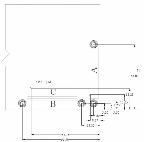
Figure HWD5: SDP-B Board Mechanical Specifications (above measurements are in mm)
resources/eval/sdp/sdp-b/hardware_description.txt · Last modified: 26 May 2016 18:58 by Eamonn Walsh