


This version (15 Feb 2022 02:24) was approved by Melissa Lorenz Lacanlale.The Previously approved version (15 Feb 2022 02:19) is available.
Table of Contents
EVALUATING THE AD9785/AD9787/AD9788 DIGITAL-TO-ANALOG CONVERTER
Preface
This user guide describes both the hardware and software setup needed to acquire data capture from AD9785-DPG2-EBZ/AD9787-DPG2-EBZ/AD9788-DPG2-EBZ evaluation board to characterize AD9785/AD9787/AD9788 12-/14-/16-bit 800Msps high-speed digital-to-analog converter.
This guide shows how AD978x-DPG2-EBZ works with SDP-H1 controller board developed by Analog Devices. Link to the previous user guide document is provided for customers who still have the DPG2 controller board.
Typical Setup
 Figure 1. EVAL-AD9785/9787/9788 Evaluation Setup
Tip: Click on any picture in this guide to open an enlarged version.
Helpful Files:
- Quick Start Guide for DPG2 users
- Data Sheet AD978x
- Schematics AD9788-DPG2-EBZ RevD
- Bill of Materials AD9788-DPG2-EBZ RevD
- PCB Gerber files AD9788-DPG2-EBZ RevD
- PCB BRD file AD9788-DPG2-EBZ RevD
- PCB Layout PDF AD9788-DPG2-EBZ RevD
Software Needed:
- DPG Lite (Recommended; Installed with ACE) or DPG Downloader
Known Issue: ACE may fail to detect HS-DAC boards, details here.
Hardware Needed:
- SDP-H1 (EVAL-SDP-CH1Z) Board
- 12V 1A Wall Wart for SDP-H1
- AD-DAC-FMC-ADP High-Speed DAC Evaluation Board to FMC Adaptor Board
- PC with ACE and DPG Lite Software Applications
- 5V 2A Power Supply
- High-Frequency Continuous Wave Generator
- Signal/Spectrum Analyzer
- (2) USB A to USB Mini Cables
- (2) SMA Cables
- (2) Banana Plug Cables
Quick Start Guide
- Make sure than on the evaluation board, JP1, JP2, JP3, and JP4 are configured such that IOUTxP and IOUTxN are connected to the corresponding baluns (T7, T8), and R8 and R9 are installed. Refer to Figure 5a.
- Configure JP5 and JP6 to connect DAC clock inputs to the desired clock source. Refer to:
- Figure 6a for direct clocking or
- Figure 6b when using AD9516.
- Attach the evaluation board to SDP-H1 FMC connector using the AD-DAC-FMC-ADP adapter board. Connect continuous wave generator for clock input to J2 (for direct clocking) or J1 (when using AD9516), and the DAC output from J4 or J8 to a signal/spectrum analyzer. Connect the evaluation board to PC via USB and to a 5V 2A power supply via banana plug cables. Refer to Figure 1.
- Connect SDP-H1 to PC via USB and to a 12V 1A power supply.
- Set clock input to:
- 400MHz and 3dBm for direct clocking, or
- 100MHz and 3dBm when using AD9516.
- Open ACE. The board will automatically be recognized by the software. Otherwise, install the plugin for AD9785/9787/9788 evaluation board.
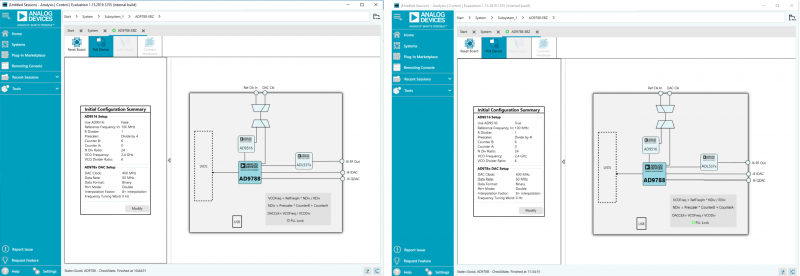 Figure 2a. ACE Initial Configuration Wizard for Direct Clocking | Figure 2b. ACE Initial Configuration Wizard when using AD9516
- In ACE,
- when AD9516 is not in use, in the wizard under “AD78x DAC Setup,” change Data Format to “Binary” and Interpolation Factor to “8x”. Click “Apply“. See Figure 2a.
- when using AD9516, check off the “Use AD9516” box. In the wizard under “AD78x DAC Setup,” change Data Format to “Binary” and Interpolation Factor to “8x”. Click “Apply”. See Figure 2b.
- Start DPG Lite or DPG Downloader. At the SDP-H1 part of the software, the device part number and DCO frequency of 50MHz should be displayed.
- In DPG Lite or DPG Downloader, from the “Add Generator Waveforms” pulldown menu, select “Single Tone” and apply the settings as shown in Figure 3. Set data rate to 50MHz and desired frequency to 10MHz. Set DAC resolution to the DAC’s number of bits (16 for AD9788, 14 for AD9787, and 12 for AD9785). Check off the “Generate Complex Data (I & Q)” box.
 Figure 3. DPG Lite session for EVAL-AD9788
- Select the in-phase tone from the “I Data Vector” pulldown menu and the quadrature tone from the “Q Data Vector” pulldown menu.
- Press the download arrow and then the play button. The FFT plot similar to Figure 4 should appear in the signal/spectrum analyzer.
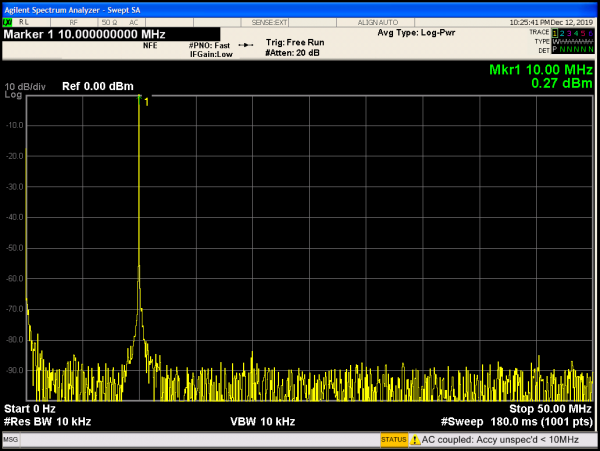 Figure 4. EVAL-AD9788 FFT for Fdac=50MHz, Fout=10MHz


Reconfiguring the Evaluation Board
Jumpers for Selecting DAC Output Configuration
By default, jumpers JP1, JP2, JP3, and JP4 are configured such that the IDAC output can be observed at SMA J4, and QDAC output at J8. See Figure 5a.
To connect to the filters that feed ADL5375, the solder jumpers need to be repositioned as shown in Figure 5b. The output from the ADL5375 Modulator can be observed at SMA J6 RF out.
 Figure 5a. DAC Outputs to Baluns (default) | Figure 5b. DAC Outputs to ADL5375 Modulator
Jumpers for Selecting the Clock Source
By default, JP5 and JP6 are configured such that DAC clock of the DUT is driven directly by an off-board clock source connected to J2. Refer to Figure 6a.
To test the performance i.e. ACLR with the clock multiplication, AD9516 is provided on board. In order to drive the DAC clock from AD9516, JP5 and JP6 needs to be changed as shown in Figure 6b. Connect the continuous wave generator to J1.
 Figure 6a. Direct clocking configuration | Figure 6b. DAC clock is driven by AD9516
Hardware Provisions for Power Supplies
There are 6 pin jumpers on the evaluation board corresponding to 6 supplies. They serve as ‘switches’ that determine if the on-board LDOs or external supplies are used for each individual supply. They are shunted by default, which means on-board LDOs are used. When an external supply is necessary, pull off the shunt from the corresponding supply and connect the external supply to the test points close to the jumper.

resources/eval/dpg/eval-ad978x.txt · Last modified: 15 Feb 2022 02:24 by Melissa Lorenz Lacanlale