


This version is outdated by a newer approved version. This version (11 Jun 2021 10:19) was approved by Shine Cabatan.The Previously approved version (07 Apr 2021 13:04) is available.
This version (11 Jun 2021 10:19) was approved by Shine Cabatan.The Previously approved version (07 Apr 2021 13:04) is available.This is an old revision of the document!
Table of Contents
EVALUATING THE AD9780/AD9781/AD9783 DIGITAL-TO-ANALOG CONVERTERS
Preface
This user guide describes both the hardware and software setup needed to acquire data capture from AD9783-DPG2-EBZ evaluation board to characterize AD9780/AD9781/AD9783 12-/14-/16- bit 500MSPS high-speed digital-to-analog converter.
This guide shows how AD9783-DPG2-EBZ works with SDP-H1 controller board developed by Analog Devices. Link to the old user guide document is provided for customers who still have DPG2 and DPG3 controller boards.
Typical Setup
 Figure 1. EVAL-AD978x Evaluation Setup
Tip: Click on any picture in this guide to open an enlarged version.
Helpful Files
- Previous Quick Start Guide for DPG2/DPG3 FPGA board.
- Data Sheet: AD978x
- Schematics: AD9783-DPG2-EBZ RevBAD9783-DUAL-EBZ RevB
- Bill of Materials AD9783-DPG2-EBZ RevB AD9783-DUAL-EBZ RevB
- PCB Gerber files: AD9783-DPG2-EBZ RevB
- PCB BRD file: AD9783-DPG2-EBZ RevB AD9783-DPG2-EBZ RevB
- PCB Layout PDF: AD9783-DPG2-EBZ RevB
Tip: Open this page in Internet Explorer to avoid problems when downloading files.
Software Needed:
Hardware Needed:
- AD9783-DPG2-EBZ Evaluation Board
- SDP-H1 (EVAL-SDP-CH1Z) Board
- 12Vdc 1A Wall Adapter for SDP-H1
- 5Vdc 1A power supply (banana plug) for the evaluation board.
- AD-DAC-FMC-ADP High-Speed DAC Evaluation Board to FMC Adaptor Board
- PC with ACE and DPG Lite Software Applications
- High-Frequency Continuous Wave Generator (Clock Source)
- Signal/Spectrum Analyzer
- (2) USB A to USB Mini Cables
- (2) SMA Cables
Quick Start Guide
- Attach AD9783-DPG2-EBZ to SDP-H1 FMC connector using the AD-DAC-FMC-ADP adapter board.
- Connect SDP-H1 to PC via USB and to a 12V 1A power supply.
- Connect the evaluation board to PC via USB and to a 5Vdc 1A power supply on P5 and P6. Refer to Figure 1.
- Connect continuous wave generator for clock input to SMA J1 and DAC output from SMA J5 (IOUT1P) or SMA J9 (IOUT2P) to a signal/spectrum analyzer.
- Set clock input to 200MHz, 3dBm.
- Open ACE. The board will be automatically recognized by the software. Click the plugin. Otherwise, install the ACE plugin for AD9783.

Figure 2. AD9783 Plugin
- On the ACE Board View, double click the AD9783 block to access the Chip View.

Figure 3. AD9783 Chip View
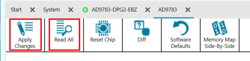
- The default values for the register is displayed and set. The values can be changed on the Chip View GUI, or on the Memory Map for registers not available in the GUI. For more info on the memory map, refer to AD978x datasheet. Once the desired values are set, Click Apply Changes and then Read All on the upper right window.

Figure 4. Apply Changes and Read All button
- Start DPG Downloader Lite. At the SDP-H1 part of the software, the device part number and clock frequency should be displayed.
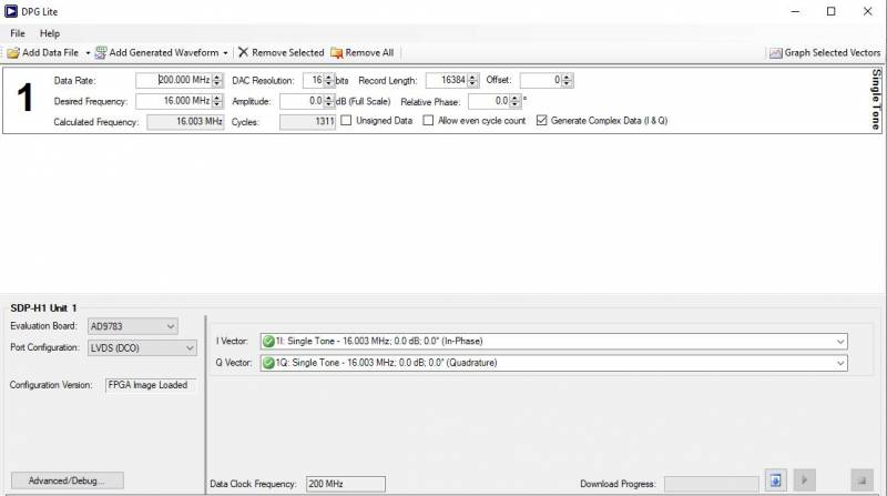
Figure 5. DPG Lite Session for EVAL-AD9783
- In DPG Downloader Lite, from the Add Generator Waveforms pulldown menu select Single Tone and apply the settings as shown in Figure 5. Set the Data Rate to 200MHz and Desired Frequency to 16MHz. Set DAC Resolution to 16 for AD9783, 14 for AD9781, and 12 for AD9780. Uncheck the Unsigned Data box and Check the Generate Complex Data (I & Q).
- Select the I/Q tone from the I/Q Data Vector pulldown menu.
- Press the download arrow and then the play button. The spectrum similar to Figure 6 should appear in the signal/spectrum analyzer.

Figure 6. Spectrum Output for AD9783; Fdac = 200MSPS, Fout = 16MHz


Using the ADL5375 Modulator
By default, solder jumpers JP4, JP5, JP6, and JP7 are configured to route the DAC outputs to SMA J5 (IOUT1P) and to J9 (IOUT2P). This jumper setting is shown on Figure 7a. To connect the DAC output to the filter that feeds into the ADL5375, the solder jumpers should be reconfigured as shown in Figure 7b. Source the desired LO of the modulator (i.e. 900 or 1800MHz, 3dBm) on SMA J2 (LO IN). The ADL5375 Modulator output can be observed on SMA J6 (RF OUT).

Figure 7a (left). DAC Output Configuration; Figure 7b (right) Modulator Output Configuration
Troubleshooting
This section lists items to check and practices to use when debugging any unexpected performance of a board. If unexpected results occur:
- Check the voltage rails of the evaluation board. P5 and P6 should be 5V; TP3, TP5, and TP7 should be 3.3V; TP9 and TP11 should be 1.8V.
- Check if all (3) blue LEDs on the AD-DAC-FMC-ADP board is lit up. Reconnect the board to the FMC connector of SDP-H1 if not lit up.
- Check if the SDP-H1 is being supplied properly by 12Vdc adaptor. Some LEDs on the SDP-H1 should lit up.
- Perform a chip reset by pressing S2 on the AD9783 evaluation board.
- Power cycle both the SDP-H1 and the AD9783 evaluation board.
- Probe C18 and C19 to make sure a clock signal is being sent into the DAC.
- Check if XD1 is lit up on the evaluation board. Reconnect/replace the USB cable connection to the evaluation board if it's not lit up.
- Disconnect and reconnect the SDP-H1 and AD9783 evaluation board. Reopen ACE and DPG Lite software.
resources/eval/dpg/eval-ad9783.1623399545.txt.gz · Last modified: 11 Jun 2021 10:19 by Shine Cabatan