


This version is outdated by a newer approved version. This version (15 Feb 2022 02:20) was approved by Melissa Lorenz Lacanlale.The Previously approved version (13 Sep 2021 09:27) is available.
This version (15 Feb 2022 02:20) was approved by Melissa Lorenz Lacanlale.The Previously approved version (13 Sep 2021 09:27) is available.This is an old revision of the document!
Table of Contents
EVALUATING THE AD9146 DIGITAL-TO-ANALOG CONVERTER
Preface
This user guide describes both the hardware and software setup needed to acquire data capture from AD9146-M5375-EBZ evaluation board to characterize AD9146 dual 16-bit 1230 MSPS TxDAC+® digital-to-analog converter.
This guide shows how AD9146-M5375-EBZ works with SDP-H1 or ADS7-V2 controller board developed by Analog Devices. Link to the previous user guide document is provided for customers who still have the DPG3 controller board.
Typical Setup

Figure 1a. EVAL-AD9146 Setup with SDP-H1

Figure 1b. EVAL-AD9146 Setup with ADS7-V2
Tip: Click on any picture in this guide to open an enlarged version.
Helpful Files:
- UG-1630 for DPG3 users
- Data Sheet: AD9146
- IBIS Model: AD9146
- Schematic: AD9146-M5375-EBZ RevA
- Bill of Materials: AD9146-M5375-EBZ RevA
- PCB Gerber files: AD9146-M5375-EBZ RevA
- PCB BRD file: AD9146-M5375-EBZ RevA
- PCB Layout PDF: AD9146-M5375-EBZ RevA
Software Needed:
Known Issue: ACE may fail to detect HS-DAC boards, details here.
Hardware Needed:
- AD9146-M5375-EBZ Evaluation Board
- SDP-H1 (EVAL-SDP-CH1Z) or ADS7-V2EBZ Evaluation Kit
- AD-DAC-FMC-ADP High-Speed DAC Evaluation Board to FMC Adaptor Board
- 5Vdc 2A Power Supply
- PC with ACE and DPG Lite Software Applications
- High-Frequency Continuous Wave Generator
- Signal/Spectrum Analyzer
- USB-A to USB-Mini Cable
- (2) SMA Cables
- The following are included in SDP-H1 Evaluation Kit:
- 12Vdc 2.5A Wall Wart
- USB-A to USB-Mini Cable
- The following are included in ADS7-V2 Evaluation Kit:
- 12V 60W AC/DC Power Supply
- Power Cord
- USB-A to USB-B Cable
Quick Start Guide
- Make sure that on the evaluation board, JP4, JP5, JP6, and JP7 are configured such that I and Q outputs are connected to the corresponding baluns (T7, T8). Refer to Figure 6. Configure JP10 and JP15 such that AD9146 clock input is connected to AD9516 clock divider/buffer. Refer to Figure 5.
- Attach the evaluation board to the FMC connector of SDP-H1 or ADS7-V2 using the AD-DAC-FMC-ADP adapter board. Connect continuous wave generator for clock input to J1, and the DAC output from J5 or J9 to a signal/spectrum analyzer. Connect the evaluation board to PC via USB and to a 5Vdc 2A power supply via banana plug cables. Refer to Figures 1a and 1b.
- If using SDP-H1, set clock input to 100 MHz and 0 dBm. Connect SDP-H1 to PC via USB and to a 12Vdc wall wart.
- If using ADS7-V2, set the clock input to 500 MHz and 0 dBm. Connect ADS-V2 to PC via USB and to a 12V 60W AC/DC power supply. Switch the board ON using S1 beside the connector for 12V supply.
- Open ACE. The board will automatically be recognized by the software. Otherwise, install the plugin for AD9146 evaluation board. Apply the configuration wizard settings shown in Figure 2a for SDP-H1 and in Figure 2b for ADS7-V2.
 Figure 2a. ACE Initial Configuration Wizard when using SDP-H1
 Figure 2b. ACE Initial Configuration Wizard when using ADS7-V2
- If using SDP-H1, set DAC frequency to 100 MHz, Interpolation to 2x and Data Format to binary format.
- If using ADS7-V2, set DAC frequency to 500 MHz, Interpolation to 2x and Data Format to binary format.
- In ACE, AD9146 on-chip PLL can be enabled or not. To enable the on-chip PLL check the Enable PLL Clock in the wizard under AD9146 PLL Setup. Select Auto Mode for PLL Mode option. The PLL Locked LED on the ACE Board View should light up green. If the LED doesn't light up, try reapplying the wizard configuration and make sure that the VCO frequency is within the valid range of 1 - 2.1 GHz.
- Start DPG Lite or DPG Downloader.
- At the SDP-H1 part of the software, the device part number and DCO frequency of around 100 MHz should be displayed.
- At the ADS7-V2 part of the software, the device part number and DCO frequency of around 500 MHz should be displayed.
- In DPG Lite or DPG Downloader, from the Add Generator Waveforms pulldown menu, select Single Tone and apply the settings as shown in Figures 3a and 3b. The data rate in DPG software should be equal to the data rate in ACE.
- When using SDP-H1, set Data Rate to 50 MHz and Desired Frequency to 10 MHz.
- When using ADS-V2, set Data Rate to 250 MHz and Desired Frequency to 21 MHz.
- Continuing on setting up DPG Lite or DPG Downloader, set DAC resolution to 16 bits. Check off the Generate Complex Data (I & Q) box.
 Figure 3a. DPG Lite session for SDP-H1
 Figure 3b. DPG Lite session for ADS7-V2
- Select the in-phase tone from the I Data Vector pulldown menu and the quadrature tone from the Q Data Vector pulldown menu.
- Press the download arrow and then the play button. The FFT plots similar to Figures 4a and 4b should appear in the signal/spectrum analyzer.
 Figure 4a. EVAL-AD9146 FFT for Data Rate = 50 MHz, Fout = 10 MHz
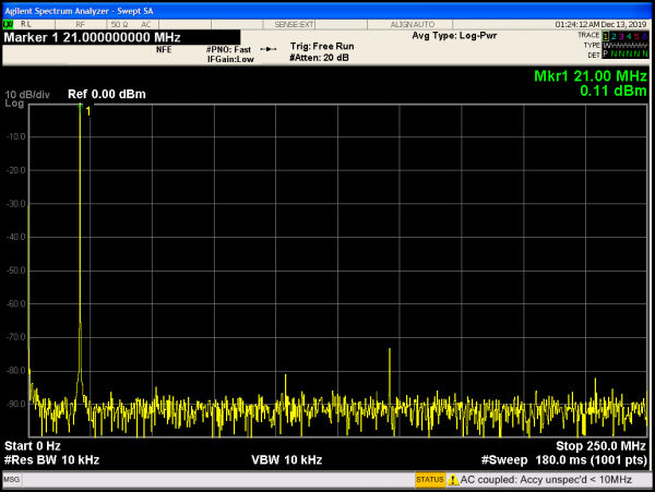 Figure 4b. EVAL-AD9146 FFT for Data Rate = 250 MHz, Fout = 21 MHz


Reconfiguring the Evaluation Board
Jumpers for Selecting the Clock Source
The AD9146 has an on-chip phase-locked loop (PLL) that uses the REFCLKP and REFCLKN pins to supply the reference clock. The AD9146-M5375-EBZ can supply the clock either from the AD9516-0 clock chip or from an additional external signal generator by connecting to J14. Connecting the inner pads to JP10 and JP15 selects the option to use the AD9146 by default, whereas soldering the outer pads chooses the external option to drive from a sine source.
 Figure 5. DAC clock input is connected to AD9516 clock divider/buffer (default)
Jumpers for Selecting DAC Output Configuration
The AD9146-M5375-EBZ evaluates both the DAC I/Q outputs as well as the modulator RF outputs. Table 1 lists the jumper configurations and the SMA connections needed to view either the DAC IF outputs or the RF outputs on the spectrum analyzer.

The evaluation board has four three pad solder jumpers, two for each DAC (IOUT1N and IOUT1P, and IOUT2 N and IOUT2P). Use these solder jumpers, JP4 through JP7, to choose between viewing the DAC output or the modulator output. By default, the jumpers are configured to view the DAC output. For the modulator, solder the inner pads.
 Figure 6. DAC I/Q Outputs to Baluns (default)
Hardware Provisions for Power Supplies
The AD9146-M5375-EBZ has five, two pin jumpers for each of the different power supplies on the board (see Table 2). By default, all of these jumpers must be populated.

Jumper for Transmit Enable pin
The AD9146 has a transmit enable feature (active low) that allows the user to control when the DACs transmit and when the outputs are clamped. This feature can be used by forcing a voltage on the TXENABLE pin via a test point. By default, the TXENABLE pin is set by the controller. Connect JP1 horizontally, as shown in Figure 7. To drive the TXENABLE pin manually, leave the jumper unsoldered.
 Figure 7. TXENABLE Pin is connected to the controller (default)
resources/eval/dpg/eval-ad9146.1644887941.txt.gz · Last modified: 15 Feb 2022 02:19 by Melissa Lorenz Lacanlale