


This version is outdated by a newer approved version. This version (01 Aug 2022 07:11) was approved by Shine Cabatan.The Previously approved version (01 Aug 2022 06:56) is available.
This version (01 Aug 2022 07:11) was approved by Shine Cabatan.The Previously approved version (01 Aug 2022 06:56) is available.This is an old revision of the document!
Table of Contents
Evaluating the AD9106/AD9102 Waveform Generator Digital-to-Analog Converter
Preface
Analog Devices is an Mbed Partner and develops code on the platform for multiple products. The AD9106 and AD9102 Mbed-enabled evaluation boards and example Mbed codes can be used as starting point for characterizing the high-speed waveform generator digital-to-analog converters before integrating them into specific applications.
This guide will focus on how AD9106-ARDZ-EBZ/AD9102-ARDZ-EBZ works with SDP-K1 controller board developed by Analog Devices. Users are not limited to using SDP-K1 for evaluation or prototyping. The evaluation boards and the example source codes with minor changes can work with other ARM-based Mbed-enabled boards. The user interface is text based.
The evaluation setup can be powered by USB only and does not require a high-frequency waveform generator for clock input. The evaluation board has an on-board 156.25 MHz crystal oscillator. To fit the evaluation system in a small form factor and manage power consumption within USB specifications, AD9106 and AD9102 supply voltages AVDD, DVDD and CLKVDD are limited to 3.3V only.
Typical Setup
 Figure 1a. EVAL-AD9106 Typical Evaluation Setup
 Figure 1b. EVAL-AD9102 Typical Evaluation Setup
Tip: Click on any picture in this guide to open an enlarged version.
Helpful Files
- Schematic: AD9106-ARDZ-EBZ, AD9102-ARDZ-EBZ
- Bill of Materials: AD9106-ARDZ-EBZ, AD9102-ARDZ-EBZ
- PCB Gerber Files: AD910x-ARDZ-EBZ Gerber Files
- PCB Board File: AD910x-ARDZ-EBZ Board File
AD910x-EBZ (Obsolete) Documentation
- Quick Start Guide: AD9106-EBZ AD9102-EBZ
- Schematic: AD9106-EBZ RevC AD9102-EBZ RevA
- Bill of Materials: AD9106-EBZ RevC AD9102-EBZ RevA
- PCB Gerber Files: AD910x-EBZ RevC
- PCB Board File: AD910x-EBZ RevC
- DAC Software Suite Update: AD9106 SPI Controller
Software Needed
- CoolTerm (Recommended) or Tera Term or PuTTy Serial Port Terminal Application
Useful Links
Hardware Needed
Minimum:
- AD9106-ARDZ-EBZ / AD9102-ARDZ-EBZ Evaluation Board
- SDP-K1 (EVAL-SDP-CK1Z) Board
- PC with Internet Connection (while using the compiler) and Terminal Application
- USB Cable for SDP-K1
- Oscilloscope
- SMA to BNC Cables
Additional:
- 7V to 12V 30W Wall Wart (if on-board amplifiers will be used)
- High-frequency Continuous Wave Generator (for clock input frequency other than 156.25 MHz)
Quick Start Guide
- Attach AD9106-ARDZ-EBZ / AD9102-ARDZ-EBZ evaluation board to SDP-K1. Make sure SDP-K1 VIO is set to 3.3V through the P14 jumper by placing the shunt on the center and 3.3V pins.
- Connect SDP-K1 to PC over USB. DS1 and DS2 on SDP-K1 and DS1 on the evaluation board should light up. Refer to Figure 1. If DAC outputs are connected to the on-board amplifiers, connect a 7V to 12V 30W wall wart to SDP-K1 DC Jack or to P15 on the evaluation board.
- Connect the outputs of the evaluation board to an oscilloscope using SMA to BNC cables. Apply the oscilloscope settings shown in the waveform captures of the example patterns in Figures 11a to 12c and 17a to 18c.

 Figure 3. EVAL-AD910x Mbed code in Analog Devices repository
- Log on to https://os.mbed.com/ then go to the EVAL-AD910x example code repository. Select the classic online compiler then click the “Import into Compiler” button as shown in Figure 3. The browser should automatically redirect to the Mbed compiler. Select SDP-K1 as development platform then import codes as program. See Figure 4.
 Figure 4. Importing code as program
- Open config.h in the Mbed compiler and define the active device. If evaluation board is AD9102-ARDZ-EBZ, uncomment line 24 by deleting the two forward slashes. Refer to Figure 5. Otherwise, proceed to compiling the code by clicking the “Compile” button.
 Figure 5. Active device selection in config.h
- As shown in Figure 6, binary code will be downloaded to the computer after successful compilation. Drag and drop this code to the SDP-K1 drive or right click the binary file then send it to SDP-K1. See Figure 7. DS1 on SDP-K1 will be blinking while the file is being sent.
 Figure 6. Successful program compilation
 Figure 7. Sending binary file to SDP-K1 drive
- After sending the code and DS1 stopped blinking, start up CoolTerm or any similar serial port terminal application. Select the com-port the SDP-K1 board is connected to. Set baudrate to 115200.
 Figure 8. CoolTerm connection settings
- Press SDP-K1 reset button. Wait for DS1 in SDP-K1 to stop blinking. Then click “Connect” on the terminal.


Figure 9a. EVAL-AD9106 Demo Program Menu | Figure 9b. EVAL-AD9102 Demo Program Menu
- Follow the application menu that will appear on the terminal window. Since the device’s clock inputs are connected to the on-board crystal oscillator and the DAC outputs to the RF transformers by default, press any key other than ‘y’ after the first two questions. Refer to Figures 9a and 9b.
- Select an option from the example summary by typing the number to left of the example description. Recommended examples for the default hardware configuration are 3 and 5 for AD9106 and 3, 5, and 6 for AD9102. To observe waveforms with frequency components outside the RF transformer’s bandwidth of 0.5-600 MHz, connect the DAC outputs to the on-board amplifiers. Refer to Table 1.
 Figure 10. Printing of SPI register addresses and data on CoolTerm
- After selecting an example, the device’s register addresses and corresponding data words will be displayed on the console and patterns will be generated at the DAC outputs as demonstrated in Figure 10. Resulting waveforms are shown in Figures 11a to 12c.


Figure 11a. AD9106 example 3 waveforms out of RF transformers | Figure 11b. AD9106 example 5 waveforms out of RF transformers
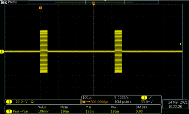

Figure 12a. AD9102 example 3 waveform out of RF transformer | Figure 12b. AD9102 example 5 waveform out of RF transformer
 Figure 12c. AD9102 example 6 waveform out of an RF transformer
- After playing one set of patterns, play another pattern or exit the program. If program is not exited after stopping pattern generation, the program will restart like in Figure 13a. Otherwise, after exiting the program like in Figure 13b, disconnecting then re-connecting to the console is needed to restart the program.


Figure 13a. Restarting the program | Figure 13b. Exiting the program


Reconfiguring the Evaluation Board
On-board jumpers and other hardware provisions are listed, and their functions described in Table 1. Meanwhile, the test points are enumerated and described in Table 2.

Using an Off-board Clock Source

Figure 14a. DAC clock is connected to on-board oscillator (default) | Figure 14b. DAC clock is connected to J10
By default, DAC CLKP and CLKN are connected to the differential outputs of the on-board crystal oscillator as shown in Figure 14a. If clock frequency other than 156.25 MHz is desired, an off-board clock source can be used and connected to J10. Change JP1 and JP2 connections first as shown in Figure 14b.
Using the On-board ADA4817-2 Amplifiers

Figure 15a. DAC ouputs are connected to RF transformers (default) | Figure 15b. DAC ouputs are connected to ADA4817-2 amplifiers

Figure 16a. SMA output connectors are connected to RF transformers (default)

Figure 16b. SMA output connectors are connected to ADA4817-2 amplifier outputs
The waveforms in Figures 11a to 12c can also be observed out of the on-board amplifiers. To do this, disconnect the DAC outputs from the RF transformers and connect them to the corresponding amplifiers as shown in Figure 15b, then disconnect the SMA connectors from the RF transformers and connect them to the amplifier outputs as shown in Figure 16b. It is expected that the amplifier output amplitudes will be higher. Lower signal amplitudes out of the RF transformers are due to insertion loss and output voltage division resulting from impedance matching between the secondary and primary sides.


Figure 17a. AD9106 example 1 waveforms out of ADA4817-2 | Figure 17b. AD9106 example 2 waveforms out of ADA4817-2


Figure 17c. AD9106 example 4 waveforms out of ADA4817-2 | Figure 17d. AD9106 example 6 waveforms out of ADA4817-2


Figure 18a. AD9102 example 1 waveform out of ADA4817 | Figure 18b. AD9102 example 2 waveform out of ADA4817

Figure 18c. AD9102 example 4 waveform out of ADA4817
To properly observe the other patterns out of the amplifiers, replace C25, C26, C54, and C55 with 0Ω resistors or remove the capacitors then solder each pair of pads together. Waveforms are shown in Figures 17a to 18c.
The common-mode voltage of the amplifier outputs can also be changed by installing resistors for DC offset correction of amplifier inputs. Refer to Table 1. Keep C25, C26, C54, and C55 pads shorted.

The on-board amplifiers can be characterized using off-board power supplies by removing E1 and E2 then connecting 5.2V 0.2A across TP5 and ground and -5.2V 0.2A across TP4 and ground.
Evaluation Board Output Interface Options
When tapping to the evaluation board outputs, users are not limited to the SMA jacks. P14 headers are provided as alternative connectors but performance is not as good as when using SMA connectors.
Using the Example Mbed Codes
The EVAL-AD910x Example Mbed Codes can be used as starting point for developing firmware for targeted applications. The codes in the repositories below demonstrates how to setup SPI communication between the ARM-based Mbed-enabled hardware, SDP-K1, and the waveform generator DACs, AD9106 or AD9102.
- Link to Program Files: https://os.mbed.com/teams/AnalogDevices/code/EVAL-AD910x/
- Link to Library Files: https://os.mbed.com/teams/AnalogDevices/code/AD910x/
To import the program files to the Mbed compiler as discussed in the Quick Start Guide, the user should have a free Mbed account and is logged on to https://os.mbed.com/. After successful program import, the user is free to use and modify the codes without violating the Analog Devices Inc. Software License Agreement in the License.txt file.
Each file and each of the functions in the files have short descriptions or briefs. This section will focus on how several files and functions can be modified using the Mbed online compiler.

Figure 19. SPI protocol definitions, example SRAM vectors, and example SPI register configurations in config.h
Setting up the SPI Interface
Aside from choosing the active device as shown in the Quick Start Guide, SPI protocol parameters particularly the clock frequency can be set at the application-level codes. Word length WORD_LEN and polarity POL need not be changed and are already set specifically for AD9106 and AD9102. Refer to Mbed OS 6 SPI Documentation for more information on these parameters.
Instructions on setting the SPI clock (SCLK) frequency are already provided in config.h as shown in Figure 19. The reason why SCLK can only be set to a number of fixed frequencies is discussed in this Mbed wiki page on SPI output clock frequency. SPI lines out of the Arduino headers or SPI1 module of the SDP-K1 ARM processor, uses 90MHz peripheral clock. Refer to these relevant source codes:

Figure 20. Device-specific I/O pins and functions declarations in ad910x.h
Initialization of digital I/O pins connected to the DAC being evaluated, and declaration of SPI register addresses and device-specific functions are in ad910x.h. See Figure 20. The functions are implemented in ad910x.cpp. The Mbed platform drivers allow setup of 4-wire SPI interface. Refer to Mbed documentation for other configurations.
Modifying SRAM Vectors
SRAM Vectors in config.h can be easily modified for a specific application. For both AD9106 and AD9102, there are 4096 addresses in the on-chip SRAM. Word length is 14 bits for AD9102, 12 bits for AD9106, and is left justified. For AD9102, data should be written in bits [15:2] and for AD9106 in bits [15:4] of each SRAM address.

Figure 21a. Waveforms that can be generated using DPG Lite

Figure 21b. Waveform vector generation using DPG Lite
Although the SRAM vectors can be modified manually, it will be more convenient to create new vectors using DPG Lite. Shown in Figure 21a are types of waveforms that can be generated using the software.
When creating data vectors for AD9106 and AD9102, make sure to choose the proper DAC resolution and leave the Unsigned Data box unchecked. A continuous wave vector with record length of 4096 can be created but the SRAM can also be composed of different types of waveforms like in the example in Figure 21b where there are 3 vectors with combined record length of 4096. These can be saved as text files and integrated into the source code.
It is not required to write to all 4096 addresses. Each DAC channel in a device can fetch data from a fixed SRAM address to another. The start and stop addresses can be set using the following registers:
- 0x5E and 0x5F for AD9102,
- 0x5E and 0x5F, 0x59 and 0x5A, 0x55 and 0x56, and 0x51 and 0x52 for AD9106 Channels 1 to 4, respectively.

SRAM data format or code follows two’s complement notation. Refer to Table 3 for the equivalent current output for an input code. 14-bit code should be shifted left by 2 bits before writing it to AD9102 SRAM while 12-bit code should be shifted left by 4 bits before writing it to AD9106 SRAM. Alternatively, 14-bit data shifted left by 2 bits can be written to AD9106 SRAM but the last two bits with be truncated. This is why in AD910x_update_sram() function in ad910x.cpp, SRAM data is by default shifted 2 bits to the left. Refer to Figure 22.

Figure 22. Function that writes to on-chip SRAM in ad910x.cpp
AD910x_print_sram() function is declared in ad910x.h and implemented in ad910x.cpp but is by default not called in the main program main.cpp. The function can be used to print in the console n number of data words from SRAM. This can be done by calling the function in main.cpp after an AD910x_update_sram().
Changing SPI Register Values
AD9106 and AD9102 have similar register maps. The latter only has less number of registers that affect device functionality because writing to registers for the 3 other DAC channels will only have an effect to AD9106. Nonetheless, the defined SPI registers address in ad910x.h will work for both devices.
The SPI register addresses were written as comment in config.h and aligned with example SPI register values for user’s convenience. Same as the SRAM vectors, these SPI register values can also be easily modified for specific applications. Refer to the device datasheets for the SPI register descriptions.
Power Supply Enable/Shutdown Pins

Figure 23. Power supply enable/shutdown pins in main.cpp
Other I/Os like the ones connected to the EN pin of the on-board oscillator supply, CVDDX, and to the SHDN_N pin of the on-board amplifier supply, LT3472, are defined in main.cpp.
As shown in Figure 23, if external or off-board clock source is chosen, en_cvddx = 0 and no power is supplied to CVDDX. If the on-board oscillator is chosen, en_cvddx = 1 and 3.3V is supplied to CVDDX.
If the user confirms that the DAC outputs are connected to the on-board amplifiers, shdn_n_lt3472 = 1 and 5.2V and -5.2V are supplied to the amplifiers provided a wall wart is connected to SDP-K1 or the evaluation board. Otherwise, shdn_n_lt3472 = 0 and the amplifiers are not powered up.
Troubleshooting
This section lists items to check and practices to use when debugging any unexpected performance of a board. If unexpected results occur
- Restart the program by stopping pattern generation and pressing “Disconnect” from the terminal window. Press “Connect” again then follow the application menu.
- Power down the whole system by disconnecting the wall wart, if using, and the USB cable from SDP-K1, then power up the system again following the steps in the Quick Start Guide.
- Measure voltages on the evaluation board. Refer to Table 2. If the voltages are off by 10% or more from the rated values, check if there are problems on component assembly or look for damaged ICs. Re-solder or replace components if necessary.
- If signal amplitude is lower than expected, compare oscilloscope settings to the recommended setup in the Quick Start Guide. Check for loose cable connections or try changing SMA-to-BNC cables. Loose connections and cable damage cause impedance mismatch.
- If there is no output at all, check if clock input to AD9106 / AD9102 is stable by measuring clock leakage. Connect one of the evaluation board outputs to a spectrum analyzer. Boards and the clock source should be powered up but the DAC should not be generating a pattern. A low-power tone should be detected at the clock frequency. Otherwise, the clock source is not properly driving the clock input pins. Try using an off-board continuous waveform generator as clock source or if already using, try increasing waveform generator output signal level to 3 dBm.
resources/eval/dpg/eval-ad9106.1659330694.txt.gz · Last modified: 01 Aug 2022 07:11 by Shine Cabatan