


This version is outdated by a newer approved version. This version (08 May 2018 19:27) was approved by Michele Viani, Annette Hurman.The Previously approved version (12 Apr 2018 20:24) is available.
This version (08 May 2018 19:27) was approved by Michele Viani, Annette Hurman.The Previously approved version (12 Apr 2018 20:24) is available.This is an old revision of the document!
Table of Contents
AD917x-FMC-EBZ Evaluation Board User Guide
What's In The Box
- AD9171-FMC-EBZ or AD9172-FMC-EBZ or AD9173-FMC-EBZ Evaluation Board
- Mini USB cable
Note: if using the KCU-105 evaluation kit as a pattern generator, an additional board is needed. Be sure to order the AD-HSDACFX3-EBZ evaluation kit as well. Customers will need to order their own KCU-105 evaluation kit from Xilinx: http://www.xilinx.com/products/boards-and-kits/kcu105.html
What's In The Box: AD-HSDACFX3-EBZ (Needed for use with the KCU-105 Only)
- FX3 Cypress Board + FMC Interconnect Board (pre-programmed and assembled for immediate use)
- Micro SD card containing FPGA image to be used with the KCU-105
General Description
The AD917x Evaluation Board Setup Guide provides details about how to set up the hardware and software for the evaluation kit. This guide explains how to setup the KCU-105 and the ADS8 and AD917x-FMC-EBZ. This evaluation kit will also support the Analog Devices ADS7 platform for lane rate configurations that are ≤12.5Gbps. The DPGDownloader software will be used to set up the data vectors and FPGA SERDES mode configuration for the KCU-105 platform, ADS8 or ADS7 and the ACE software (Analysis | Control | Evaluation) will be used to set up the AD917x evaluation board, including the HMC7044 clock distribution chip on the board. The AD917x-FMC-EBZ evaluation board can be driven by an external direct clock with DAC PLL off or the on-board clock from HMC7044 with DAC PLL on. The reference clock of HMC7044 can be provided by the on-board 122.88MHz crystal or the external signal generator.
Software Installation
The required software to run the evaluation board is as follows:
- DAC Software Suite: https://wiki.analog.com/resources/eval/dpg/dacsoftwaresuite
- ACE (Analysis|Control|Evaluate): https://wiki.analog.com/resources/tools-software/ace
Once both programs are installed, launch ACE. On the start-up window, navigate to Tools → Manage Plugins. The plugin manager pop-up window will display. Search for AD9172 and select install plugin to install the appropriate plugin files for the FMC evaluation board.
Hardware Setup
The following items should be included in the evaluation kit (KCU-105 platform not included, purchased separately by the customer):
- Interconnect Board (connects FX3 board to the KCU-105 FMC connector) with Cypress FX3 board (only needed if using the KCU-105)
- USB2.0 Cable (connects FX3 board to USB port on a computer)
- AD917x-FMC-EBZ Evaluation Board
- Mini USB to USB Cable (connects mini USB port on evaluation board to USB port on a computer)
- MicroSD card with preprogrammed FPGA image to be used with DPGDownloader software (not needed for ADS7 or ADS8)
Connect the boards and cables to the KCU-105 board as shown in Figure 1 below.
 Figure 1. Evaluation Board Kit Components Hardware Connection Setup
Connect a reference clock frequency to the “Board Ref Clock” connection shown in Figure 1 (SMA connector J4). This is the configuration required any time the evaluation board is to be measured and used. Turn on the KCU-105 power and plug in both USB cables to the host computer.
Additional KCU105 Setup
The KCU-105 board requires some additional setup steps to be compatible with the DPGDownloader software. A Micro-SD card that contains the FPGA image used with DPGDownloader is included in the evaluation kit. Before powering on the KCU105 unit, this Micro-SD card should be inserted into the appropriate slot on the bottom right-hand side of the KCU105 evaluation board as shown in Figure 1. In order to boot up the KCU105 board using the image from the Micro-SD card, ensure that the DIP switch settings on SW15 are set according to Figure 2 below.
 Figure 2. KCU105 DIP Switch Settings for Loading Image from Micro-SD Card
Once these steps are complete, the KCU105 board can be powered on and plugged into the USB ports on the host PC. This step only needs to be done once in order to set up the FPGA board properly for any future use with DPGDownloader software.
ADS7/ADS8 Setup
The Cypress FX3 and interconnect board are not needed if the ADS7 or ADS8 board is used for data pattern generation. The hardware setup configuration when using the ADS7/ADS8 is as follows:
- Connect the AD917x-FMC-EBZ board to the FMC connector on the ADS7 or ADS8.
- Plug the mini USB cable into the AD917x-FMC-EBZ board and connect the other end to the PC being used.
- Connect the ADS7 or ADS8 to the PC being used with the USB cable to the ADS7 or ADS8 board and connect the power supply.
- Connect the DAC0 output (J2) or the DAC1 output (J1) to the spectrum analyzer.
 Figure 3. Evaluation Board Kit Components Hardware Connection Setup with ADS8
Direct Clock the AD917x
For some configurations, the DAC on-chip PLL may not support the desired DAC sampling clock. In order to direct clock the CLK± pins of the AD917x, rotate C36 and C38 to instead be populated on C34 and C35 as shown in the Figure 4. Connect a high-performance clock with >=12dBm output level to J34 for the direct clock option. A second low phase noise, high frequency clock source (3.84MHz , 7.68MHz, 15.36MHz, 30.72MHz, 61.44MHz, 122.88MHz, 245.76MHz and 491.52MHz) with 0 dBm output level that is the reference clock of the HMC7044 should be connected to the SMA connector J41; the two clock sources should be synchronized through the 10MHz INPUT/OUTPUT port in the back panel. A unit such as the Rohde and Schwarz SMA100 has a convenient option for a secondary signal source, and using it will ensure the two clocks are synchronized.
 Figure 4. Direct Clocking Option for DAC Clk± Pins
DC Test/NCO Mode Without ADS7/ADS8/KCU105
The AD917x can work in DC TEST/NCO mode without ADS7/ADS8/KCU105 in non-(1x-1x) operating modes, but it has to run from an external power supply. In this case, DO NOT CONNECT the AD917x-FMC-EBZ board to the ADS7/ADS8/KCU105. Instead, connect +12V to TP41 (red), GND to TP42 (black). The external power supply should have capacity for 1A of current. Put the jumper on JP71 for powering on the PIC and USB port. If using an external clock source, connect a low phase noise, high frequency clock source to J34. In addition, connect the spectrum analyzer to the SMA connector, J1 or J2.
Using DPGDownloader Software
Launch the DPGDownloader software from the Start Menu (Start → All Programs → Analog Devices → DPG → DPG Downloader). When the program starts the DPG Panel should look recognize the evaluation board connected as shown in the AD917x panel being displayed as shown in Figure 5. The desired SERDES JESD204B mode can be selected by using the “JSED Mode” drop-down menu. If running in Dual Link mode, check the “Dual Link” checkbox on the panel to enable the second link options. Use the “Add Generated Waveform” drop-down menu to create vectors to send to the evaluation board as desired. Note: If using the KCU-105, first power up the KCU105 board and wait for the heartbeat LEDs shown in Figure 1 to begin flashing. Then open up DPGDownloader and ensure the Configuration Version displays 11/07/16, confirming that the FPGA image is loaded properly from the microSD card. If this does not display or if the KCU105 has been powered off and back on again, reselect the AD917x from the Evaluation Board dropdown menu to reinitialize the panel and the configuration version should display properly.
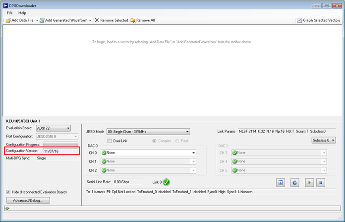 Figure 5. DPGDownloader AD917x Panel
Depending on the JESD Mode selected, different combinations of channels and DAC selection options become active on the GUI and allow for user input. The “Link Params” readback displays the JESD204B link parameters that are configured in the FPGA. The following GUI button controls operate as follows:
 Stops playing the current vector in memory and downloads the selected vectors in each channel drop-down selection
 Resynchronizes the SERDES PLL band based on the Serial Line Rate detected – needed every time the lane rate changes for a different configuration or the SERDES clock glitches due to reprogramming of the HMC7044
 Plays the selected vectors in each channel drop-down selection
 Stops the selected vectors in each channel drop-down selection from playing
Loading Custom Vectors
If a custom vector is to be used, the format of this vector will depend on the mode of operation chosen. If the mode chosen is a real mode (will display which mode type it is in the DPGDownloader panel), create separate I and Q vectors as desired and load them in individually to the desired DAC channels. If the mode chosen is a complex mode, the vector loaded into DPGDownloader should be one single vector that first has the I vector data then concatenate the Q vector data all into one file. Load this vector into the panel and then select the complex concatenated vector into the desired DAC channels.
Using ACE Software
Plugin Installation
To get the AD917x plugins, launch the ACE software from the Start Menu (Start → All Programs → Analog Devices → ACE → ACE) and select “Tools” → “Manage Plugins” or click the 'Plugin Manager Icon' in the bottom right-hand corner of the ACE application, shown in Figure 6. This will launch the plugin manager in ACE.
 Figure 6. ACE Plugin Manager
In the plugin manager, look under “Available Packages” for the Board.AD9172 plugins, select it and click “Install Selected”, shown in Figure 7.
 Figure 7. Install AD917x Board Plugins
Once the installation finishes click “Close” and you should see the AD917x-FMC-EBZ board plugin show up in the offline area for “Explore Local Plugins”. If the evaluation board is connected through USB, the ACE GUI should look recognize the AD917x-FMC-EBZ evaluation board connected as shown in Figure 8 in the “Attached Hardware” section. If it does not recognize the board immediately, try closing ACE after the installation is complete and relaunching and the software should bring up the board plugin with the version of the plugin that was installed displaying (Version 1.2.1.0 in this example shown).
 Figure 8. ACE Software GUI
Board Plugin
 Figure 9. AD917x-FMC-EBZ Board Plugin View with Startup Wizard
By double-clicking on the AD917x-FMC-EBZ icon the board plugin view will be automatically displayed, as shown in Figure 9.The board view contains an easy Startup Wizard which allows the user to choose the different configurations for how to set up the AD917x (along with the HMC7044 clock chip) easily without manually programming the part. It supports both DC Test Mode functionality as well as SERDES interface functionality. The various sections of the wizard can be expanded or collapsed by pressing the ![]() or
or ![]() buttons.
The following GUI inputs are defined as follows:
buttons.
The following GUI inputs are defined as follows:
Board Clock Settings:
- AD917x Clock Source: this dropdown lets the wizard know whether you are using the HMC7044 to supply the clock to the CLK± pins of the DAC or if you are directly clocking the DAC using J34 input. The direct clock option may be required if you are using a DAC clock frequency that is not covered by the internal PLL range (8.74GHz to 12.42GHz VCO with divide by 1, 2 and 3 options) or that is outside the supported output frequency range of the HMC7044 (maximum output is 3.2GHz).
- AD917x Ref Clock: drop-down menu for available DAC reference clock frequencies. If the desired reference clock is not listed, choose “Other frequency” and type in the value in the AD917x PLL Manual Ref Clock field.
- HMC7044 PLL1 Ref Clock Source: this dropdown lets the wizard know whether you are using the on-board 122.88MHz crystal to supply the clock to the HMC7044 PLL1 or if you are directly providing the reference clock to the HMC7044 using J41 input.
- HMC7044 PLL1 Ref Clock: drop-down menu for available PLL1 Ref clock frequencies. Select the frequency value and supply this clock as the external HMC7044 reference clock using J41 input.
- Direct Clock Source: this dropdown lets the wizard know whether you are using the external signal generator or HMC7044 to clock the DAC.
DC Test Mode:
- Enable DC Test Mode: checkbox enables the use of the DC test mode inside the part, the appropriate number of channel DC value inputs will be enabled based on the SERDES Link Mode and JESD Mode selections made in the ‘SERDES Interface’ section of the GUI.
- Channel x DC Value ( dB ): user inputs dB value for the DC value per channel
SERDES Interface:
- Link Mode: select Single Link or Dual Link depending on the mode desired, ensure the same setting is done on the DPGDownloader panel
- JESD Mode: depending on whether Single Link or Dual Link is selected, certain JESD Modes (as defined in the datasheet) will be available
- Channel/Datapath Interpolation: depending on the JESD Mode selected the channel/main datapath interpolation options will update to valid options for that given mode (as defined in the datasheet)
Clock Frequencies (Data/DAC/Lane Rates):
- Input Data Rate/Max Data Rate: user inputs desired data rate for the configuration (must be integer multiple of the HMC7044 Clock Input frequency selected) and must be less than the calculated Max Data Rate readback.
- DAC Clock Rate/Lane Rate: calculated readbacks of the DAC rate and lane rate based on the above user input selections
- Clock Output Divider: these are options for what clock output frequency is desired for the clock output driver coming out of J3. The clock output is DAC Clock÷Clock Output Divider chosen.
DAC PLL:
- PLL En: if the DAC clock rate is within the DAC PLL coverage range, the DAC PLL will be enabled. The readback in the wizard will display “True” if the PLL is being used or “False” if the PLL is bypassed (the DAC clock falls out of the ranges of the PLL VCO bands).
- DAC Ref Clock: the clock frequency thatis being used as the reference clock for the DAC PLL and sent to the CLK+/- pins of the DAC. This value will match the chosen value from the AD917x PLL Ref Clock control in the ‘Board Clock Inputs’ section of the wizard.
- Divisor_M/Divisor_N: DAC PLL dividers that are calculated based on the reference clock and DAC clock frequencies automatically.
NCO Frequency Controls:
- Depending on the JESD Mode selected, the appropriate number of channel and main datapath NCOs will be enabled for user input. These frequency shift values should be inputted as a frequency value (ie 1.84GHz) not as the raw FTW values for the SPI programming – calculations are done automatically for the user
Digital Gain Controls:
- Depending on the JESD Mode selected, the appropriate number of channel digital gain controls will be enabled for user input. These gain values should be inputted as a dB values (ie. -6dB) not as the raw gain code values for the SPI programming – calculations are done automatically for the user. Note the gain block is not available when using 1x channel interpolation.
SERDES Readback Parameters:
- Depending on the JESD Mode selected, the some of the SERDES parameters for the link establishment are displayed for user reference.
After the wizard parameters are configured as desired, hitting “Apply” runs the startup routine for the part and configures the evaluation board. Clicking the “Read SERDES Status” button on the board diagram reads back the link status registers for CGS, Frame Sync, Good Checksum, and ILAS per link and logical lane. The Macro Tool can be used to record the startup sequence executed by the wizard. Before hitting “Apply” click the “Record” button () in the Macro Tool editor (ensure “Record Sub-Commands” is checked) and then hit “Apply”. Once the sequence is finished running a printout of the register writes to each of the parts is displayed. This recorded macro can be saved to a file and then the Macro to Hex Converter Tool (located in Start → All Programs → Analog Devices → ACE → Tools → Macro to Hex Converter) can be used to convert the cumbersome .acemacro file into an easy-to-read text file with the simple register read/write functions.
Chip Plugin
By double-clicking on the AD917x plugin on the board diagram the software will navigate down to the AD917x chip view displaying a non-interactive block diagram view representative of the functional block diagram of the part, as shown in Figure 10. By clicking the “Proceed to Memory Map” button in the bottom right hand corner the Memory Map view will be displayed and the full register map can be viewed. Using the Functional Group menu along the left hand side displays groups of controls according to functionality for a filtered view of the SPI map controls, as shown in Figure 11.

Figure 10. AD9172 Chip View

Figure 11. AD9172 Memory Map View
ACE Macro Recorder Tool
ACE also contains the Macro Tool, which can be used to record register reads and writes. This is executed in the memory map view or with the initialization wizard. To use, check the “Record Sub-Commands” checkbox and press the record button. Changes in the memory map, which are bolded until they are applied to the part, are recorded as UI commands by the macro tool once the changes are made. Changed register write commands for the controls are also recorded. Hit “Apply Changes” to execute the commands and make changes in the memory map. To stop recording, click the “Stop Recording” button. A macro tool page with the command steps will be created. The macro can be saved using the “Save Macro” button so that it may be loaded for future use.

Macro tool in ACE example view. The Stop Recording, Record, and Save Macro commands are located at the top of the macro tool.
The raw macro file will be saved using ACE syntax, which is not easily readable. To remedy this, the ACE software download includes the Macro to Hex Conversion Tool. The user can choose to include or exclude register write, reads, and/or comments in the conversion. The file pathways for the source and save paths should be the same, except that one should be an .acemacro file and the other should be a .txt file. The “Convert” button converts and opens the converted text file, which is easier to read. The conversion tool can also convert back to an .acemacro file if desired. The Macro to Hex converter tool is located in the start menu under “All Programs” --> “Analog Devices” --> “ACE” --> “Tools”.


Conversion set-up for macro to hex
Converted text file
For more information about ACE and its features, visit https://wiki.analog.com/resources/tools-software/ace.
Example Software Setup Procedure
The following steps show how to set up the AD917[2,3]-FMC-EBZ evaluation board in the conditions below:
- Dual Link Mode
- JESD Mode 4 (Dual Band Mode: M = 4, L = 4, S = 1, F = 2)
- Channel Interp: 3x
- Datapath Interp: 8x
- Input Data Rate: 491.52MHz
- PLL Reference Clock Frequency: 122.88MHz
- Channel NCO Shifts: ±152.5MHz
- Final NCO Shifts: 1.9875GHz
- Input Signal: Multi-tone ±37.5MHz, Multi-tone ±30MHz
- DAC Rate:11.79648GHz
- SERDES Lane Rate: 9.8404Gbps
Begin by connecting the hardware according to Figure 1 and powering up the FPGA board. Connect an SMA cable from J2 or J1 to a spectrum analyzer to measure the performance of DAC 0 or DAC1. Launch DPGDownloader from the Start Menu and add two multi-tone vectors at each of the pair of desired frequencies with the following parameters:
- Data Rate: 491.52MHz
- Amplitude: -10dB
- Generate Complex Data ( I & Q ): Checked
- Desired Frequencies: ±37.5MHz, ±30MHz
- Unsigned Data: unchecked
From the JESD Mode drop-down, select mode 1 and check the “Dual Link” checkbox. For each of the channel input drop-downs select the single-tone vector generated. All these settings should be configured as shown in Figure 12.
 Figure 12. DPGDownloader Panel Setup
Launch ACE from the Start Menu and configure the wizard as listed below and shown in Figure 13 and Figure 14:
- Default Board Clock Setting
- JESD Mode: 4
- Dual Link Mode
- Channel Interp: 3
- Datapath Interp: 8
- Input Data Rate: 491.52MHz
- NCO Controls: Channel 0: -152.5MHz, Channel 1: +152.5MHz, Final NCO 0: 1.9875GHz, Channel 3: -152.5MHz, Channel 4: +152.5MHz, Final NCO 1: 1.9875GHz
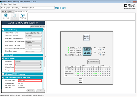 Figure 13. AD9172-FMC-EBZ ACE Wizard Setup
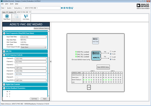 Figure 14. AD9172-FMC-EBZ ACE Wizard Setup
In ACE, hit “Apply” and let the sequence finish running. Then in DPGDownloader hit “Stop”, then “Download”, then “Resync”, then “Play” (should always be this order when downloading a vector or setting up the link) and the links should go high and the Serial Line Rate on the GUI should read 9.8304Gbps, as seen in Figure 15.
 Figure 15. DPGDownloader Panel with Links Established
In ACE, hit the “Read SERDES Status” button on the board view and the readbacks should display that the JESD PLL, DAC PLL and both Logical Lane 0 and 1 on both links are high for all flag readbacks, as shown in Figure 16.
 Figure 16. AD9172-FMC-EBZ ACE Setup with Links Established
When looking at the spectrum, there should be tones at 1.9875GHz - 152.5MHz ± 37.5MHz = 1797.5MHz and 1872.5MHz for one band and 1.9875GHz + 152.5MHz ± 30MHz = 2110.0MHz and 2170.0MHz for the second band as shown in Figure 17.
 Figure 17. AD9172-FMC-EBZ DAC0 Spectrum Output for Dual Band Case
resources/eval/dpg/ad917x-fmc-ebz.1525800362.txt.gz · Last modified: 08 May 2018 19:26 by Michele Viani