 This version (30 Sep 2016 23:35) was approved by Dan Fague.The Previously approved version (06 Jul 2016 15:04) is available.
This is an old revision of the document!
The AD916x-FMCx-EBZ EVB connects to an ADS7-V1 or ADS7-V2 Pattern Generator to allow for quick evaluation of the AD916x, a high-speed, RF Digital to Analog converter (RF DAC). The ADS7 automatically formats the data and sends it to the AD916x EVB, simplifying evaluation of the device. The Evaluation Board (EVB) runs from the FMC power supply. The AD916x-FMCx-EBZ EVB can be driven by an external clock or the on-board clock, the ADF4355, as shown in Figure 1. There is a single pole, double throw (SPDT) switch on the board for selecting the clock source. Figure 2 is an image of the top side of the AD916x-FMCx-EBZ. The board includes a clock buffer, the AD9508, which provides the reference clock and SYSREF to the ADS7 and the SYSREF signal to DAC.
The AD916x-FMCx-EBZ Evaluation Board software has an easy-to-use graphical user interface (GUI) called ACE (Analysis, Control, Evaluation). It is included on the Evaluation Board CD. This will install DPG Downloader (for loading vectors into the ADS7) and the AD916x ACE SPI programmer application. The SPI programmer enables full access to the AD916x’s register map, and has additional functionality such as the ability to record, load, and save macros, or register sequences, to ease programming of the device. The ADF4355 and AD9508 are also configured by ACE. Several macros or register sequences will be used by this guide to demonstrate the usefulness of the function and to ease the setup of the device. ACE also controls the SPDT switch for selecting the clock source.
 Figure 1. Block diagram of the AD916x-FMCx-EBZ lab bench set-up
 Figure 2. Top view of AD916x-FMC-EBZ Evaluation Board
Remove the jumper on JP1. A low phase noise, high frequency clock source should be connected to the SMA connector, J31; and output level set to 0dBm. A second low phase noise, high frequency clock source (10MHz to 250MHz) with 0 dBm output level that is the reference clock of the ADF4355 should be connected to the SMA connector J61; the two clock sources should be synchronized. A unit such as the Rohde and Shwarz SMA100 has a convenient option for a secondary signal source, and using it will ensure the two clocks are synchronized. Or, the 10 MHz reference output of the signal generator can be used as the reference input. The spectrum analyzer should be connected to the SMA connector, J32. Affix the AD916x-FMCx-EBZ Eval board to the ADS7-V1 using the FMC connector closer to the corner of the boar8. The ADS7-V2 has a single FMC connector and the AD916x-FMCx-EBZ Eval board should be connected to it.
Figure 3. View of the top of the ADS7-V1 pattern generator board
Figure 4. View of the top of the ADS7-V2 pattern generator board
Put the jumper on JP1. And connect the spectrum analyzer to the SMA connector, J32. Affix the AD916x-FMCx-EBZ Eval board to the ADS7-V1 using the FMC connector closer to the corner. The ADS7-V2 has a single FMC connector and the AD916x-FMCx-EBZ Eval board should be connected to it.
The AD9162 and AD9164 can work in DC TEST/NCO mode without the ADS7, but it has to run from an external power supply. In this case, DO NOT CONNECT the AD916x-FMCx-EBZ board to the ADS7. Instead, connect +12V to TP41 (red), GND to TP64 (black). The external power supply should have capacity for 1A of current. Put the jumper on JP1 if using the on-board ADF4355 as the clock source. If using an external clock source, connect a low phase noise, high frequency clock source to J31. And connect the spectrum analyzer to the SMA connector, J32. The PC should be connected to the EVB using the mini-USB connector XP2 after installation of the Evaluation Board software. Do not connect the USB cable until after the software has been loaded onto the PC.
The PC software comes on the included Evaluation Board DVD. The installation will include an updated version of the DPG Downloader software as well as all the necessary AD916x-FMCx-EBZ files including schematic, board layout, data sheet, SPI programmer, and other files.
Initial Set-Up
Install the DPG Downloader and AD916x software and support files on your PC by running the “autorun.exe” program. It will appear as in Figure 5. Run both of the indicated files, one for the DAC Software Suite and the other for the ACE installer.
 Figure 5. Entry screen of the installer program for the DAC Software Suite and ACE installer
It is suggested that the basic set-up is verified before making any modifications to the evaluation board. Several different configurations and scenarios will be described in this User guide, with step-by-step instructions for each one of them. Not all need to be completed, but rather choose the scenario(s) which is/are desired to be evaluated and follow the instructions. A summary software User’s Guide is at the end of the start-up scenarios.
The spectrum analyzer can be configured with Start Frequency = 50 MHz, Stop Frequency 5 GHz, and Resolution Bandwidth of 300 kHz. Use an Average/RMS detector setting, and choose Input Attenuation to be 6 dB. This can be adjusted later if indications are that the analyzer is causing degradations (warnings on the analyzer itself, or third order products appearing on the output spectrum.).
1. Open the ACE software, which is located in Start→Programs→Analog Devices→ACE→ACE. The screen will appear similar to Figure 6 below. ACE is the software that is used to load the registers in the AD916x. The ACE software enables full access to the AD916x register map, and also has several views and features that simplify its use. Many of the ACE software features will be covered in the ACE Software User’s Guide section. This section will focus on what is necessary to start-up the AD916x in DC TEST/NCO mode.
 Figure 6. The entry screen of the ACE SPI programmer software
2. Open the board view by double clicking on the AD916x Eval Board area, then select clock source “ADF4355-ADCLK914” as shown in Figure 7.
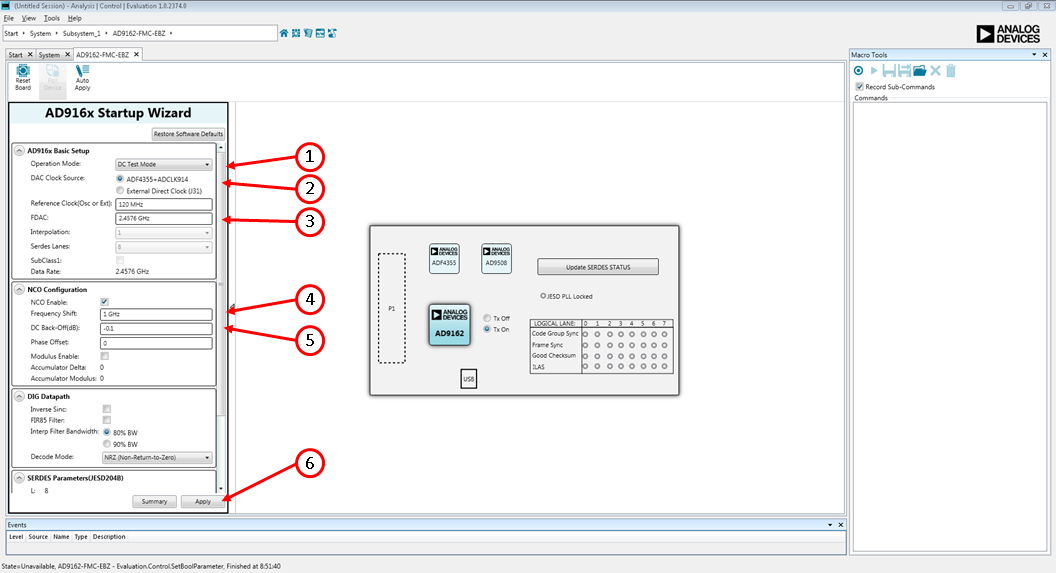 Figure 7. AD916x Eval Board View and Clock Source Selection in ACE
3. Using the AD916x Startup Wizard on the left side of the screen, do the following:
A 1 GHz single tone should now appear on the spectrum analyzer as shown in Figure 8. Change the NCO frequency and repeat Step 3 to select a different output frequency.
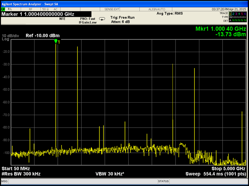 Figure 8. Spectrum Analyzer plot of DAC output in NCO mode, showing single tone at 1 GHz
4. To avoid the startup sequence each time, the icon for the AD916x can be double clicked, and the Device View will be displayed, as shown in Figure 9. The Device View is an interactive view of the AD916x that enables the user to easily configure the more common features of the device, including the NCO (highlighted) and the FIR85 enable (also highlighted), the DAC decode mode, and the clock input tuning parameters (if needed). After entering a number or selecting an option or clicking on a block to enable or disable it, click the “Apply Changes” button in the top left corner of the screen to apply the changes to the device’s registers.
Configure the hardware according to the hardware set-up instructions given in the Hardware Setup section above. The spectrum analyzer can be configured with Start Frequency = 50 MHz, Stop Frequency 5 GHz, and Resolution Bandwidth of 300 kHz. Use an Average/RMS detector setting, and choose Input Attenuation to be 6 dB. This can be adjusted later if indications are that the analyzer is causing degradations (warnings on the analyzer itself, or third order products appearing on the output spectrum.). Load and Play Pattern to the ADS7 Open DPGDownloader (Start > Programs > Analog Devices > DPG > DPGDownloader). Ensure that the program detects the AD916x, as indicated in the “Evaluation Board” drop-down list, and select it. For this evaluation board, JESD204B is the only valid Port Configuration, and it will be selected automatically. The “Lane Rate” window may not yet show a clock frequency, but it normally does. In the lower portion of the screen, choose Subclass ‘0’. The screen should look like Figure 10. The SYNC Status may show a Green check mark or a Red “X”. It is irrelevant at this point.
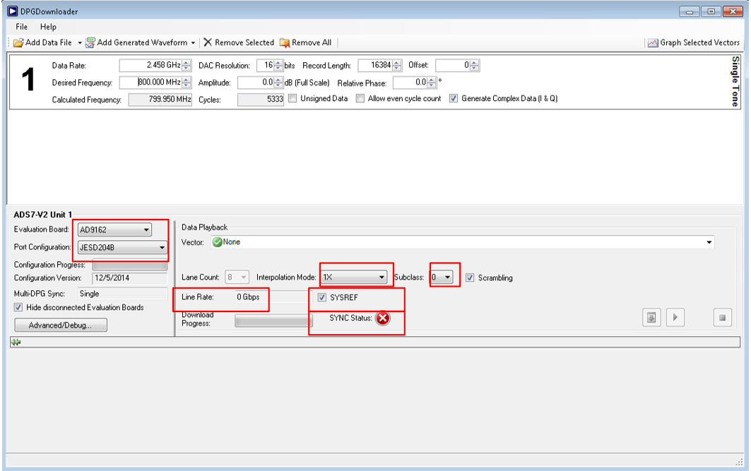 Figure 10. Initial screen of DPG Downloader when configured for AD916x
Click on “Add Generated Waveform”, and then “Single Tone”, as shown in Figure 11. A single tone panel will be added to the vector list. Enter the sample rate, or DAC clock frequency in this case, 2.4576 GHz. Next, choose the “Resolution” to be 16 bits. Choose a center frequency of 800 MHz. Keep “Amplitude” as 0 dB. Uncheck the “Unsigned Data” check box because the AD916x only accepts 2’s Complement data. The signal should appear on the list of signals as shown in Figure 11. Be sure “Generate Complex Data (I & Q)” is NOT checked.
The AD9161 resolution is 11 bit and the AD9162, AD9163, and AD9164 resolutions are 16 bit. The AD9161 can receive either 16-bit or 11-bit data because the JESD data packing engine packs data in 8-bit size. So, if 11-bit data is chosen, the DPG Downloader software will zero-pad the data words to create 16-bit words for transfer to the data framer. Since the AD9161 datapath is 16-bits, it is recommended that 16-bit data is sent to the device so that true 16-bit math can be computed, with truncation happening prior to the DAC decoder. Sending 16-bit data this way will slightly improve spurious performance as compared to sending 11-bit data.
 Figure 11. Choose “Single Tone” as the vector type
Next, in the lower portion of the screen, select “”1: Single Tone – 799.950 MHz; 0.0 dB; 0.0o” as the Data Vector. The other options can be left at their default values. The “SYNC Status” may show as the red “X” as in Figure 12.
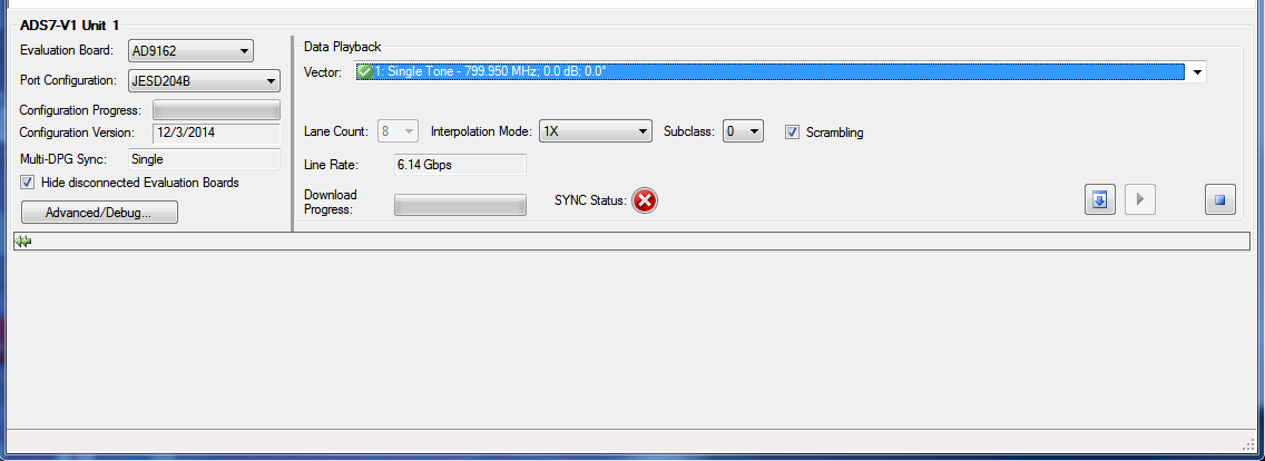 Figure 12. DPG Downloader Lower section, used to select the desired vector and download it to the ADS7 unit
Make sure the ADS7 unit is powered up and the AD916x eval board is plugged into it correctly. Click the button to download the pattern from the computer to the ADS7 unit, wait for the Play ( ) button to become active, and then click the Play ( ) button to begin vector playback to the AD916x.
1. Open the ACE software, which is located in Start→Programs→Analog Devices→ACE→ACE. The screen will appear similar to Figure 13 as below. ACE is the software that is used to load the registers in the AD916x. The ACE software enables full access to the AD916x register map, and also has several views and features that simplify its use. Many of the ACE software features will be covered in the ACE Software User’s Guide. This section will focus on what is necessary to start-up the AD916x in JESD mode.
 Figure 13. The entry screen of the ACE SPI programmer software
1. Open the board view by double clicking on the AD916x Eval Board area, then select clock source as shown in Figure 14.
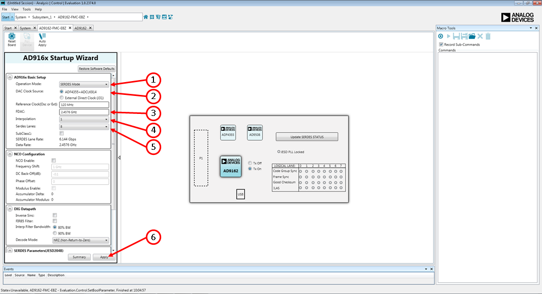 Figure 14. AD916x Eval Board View and Clock Source Selection in ACE
2. For this example, the NCO will not be used. Using the AD916x Startup Wizard, on the left side of the screen, do the following:
3. The Lane Rate frequency from the AD916x should be reported in DPG Downloader as 6.144 Gbps as shown in Figure 15. The “SYNC Status” should show as the green check mark.
 Figure 15. Download single tone and play it
4. An 800 MHz single tone should now appear on the spectrum analyzer as shown in Figure 16.
 Figure 16. Spectrum Analyzer plot of DAC output in JESD 8-lane, 1x mode, showing single tone at 800 MHz
5. The frequency of the tone can be changed either by
The re-download may momentarily bring the JESD link down, but the link should recover and re-sync and the new output frequency should be observed on the spectrum analyzer.
6. Other vectors can also be generated and downloaded in a similar manner once the JESD link is up.
7. If the user want to run new setting like different clock rate, interpolation ratio, lanes and reference clock, just go to “AD916x_Initial_Worksheet.xlsx”, repeat step 2 to step 7.
8. For debugging suggestions in case the link does not come up, see the Errors section.
9. If the interpolation ratio configured in the “AD916x_Initial_Worksheet.xlsx” is bigger than 1, DPG Downloader configuration shall be changed as well as shown in Figure 17 . The data type is complex and interpolation mode is set to “>1x”.
 Figure 17. DPG Downloader when configured for interpolation ratio >1
The DPG Downloader software allows users to import and use files generated outside the tool. To do this,
1. Generate a file with the following criteria:
2. Import the file into DPG Downloader by choosing the “Add Data File” button below the “File” menu, and selecting the desired text file. (See Figure 18.)
3. Select and download this file as with any other signal file. Note that an in-phase (I) and quadrature-phase (Q) file must be generated for any of the complex data modes.
The differences between the AD9161, AD9162, AD9163, and AD9164 FMC boards are the DAC, package, and its output Balun as shown in Table 1. For example, the AD916x-FMCx-EBZ uses the Marki BAL-0009SMG and the AD916x-FMCB-EBZ uses the Mini-Circuits TC1-1-43A+.
Table 1 AD916x boards differences
| Board PN | DAC | DAC Package | Output Balun | |
|---|---|---|---|---|
| 1 | AD9162-FMC-EBZ | AD9162 | 165-Ball, 8mm x 8mm CSP-BGA with 0.5mm pitch | Marki BAL-0009SMG |
| 2 | AD9164-FMC-EBZ | AD9164 | 165-Ball, 8mm x 8mm CSP-BGA with 0.5mm pitch | Marki BAL-0009SMG |
| 3 | AD9162-FMCB-EBZ | AD9162 | 165-Ball, 8mm x 8mm CSP-BGA with 0.5mm pitch | TC1-1-43A+ |
| 4 | AD9164-FMCB-EBZ | AD9164 | 165-Ball, 8mm x 8mm CSP-BGA with 0.5mm pitch | TC1-1-43A+ |
| 5 | AD9161-FMCC-EBZ | AD9161 | 169-Ball, 11mm x 11mm CSP-BGA with 0.8mm pitch | TCM1-63AX+ |
| 6 | AD9162-FMCC-EBZ | AD9162 | 169-Ball, 11mm x 11mm CSP-BGA with 0.8mm pitch | TCM1-63AX+ |
| 7 | AD9163-FMCC-EBZ | AD9163 | 169-Ball, 11mm x 11mm CSP-BGA with 0.8mm pitch | TCM1-63AX+ |
| 8 | AD9164-FMCC-EBZ | AD9164 | 169-Ball, 11mm x 11mm CSP-BGA with 0.8mm pitch | TCM1-63AX+ |
The insertion loss, the phase mismatch and the amplitude mismatch of these Baluns are different at the each frequency, so the DAC output fundamental amplitude response and the spurious levels can be slightly different. The typical fundamental amplitude responses (without the cable loss calibration) are shown in Figure 18.
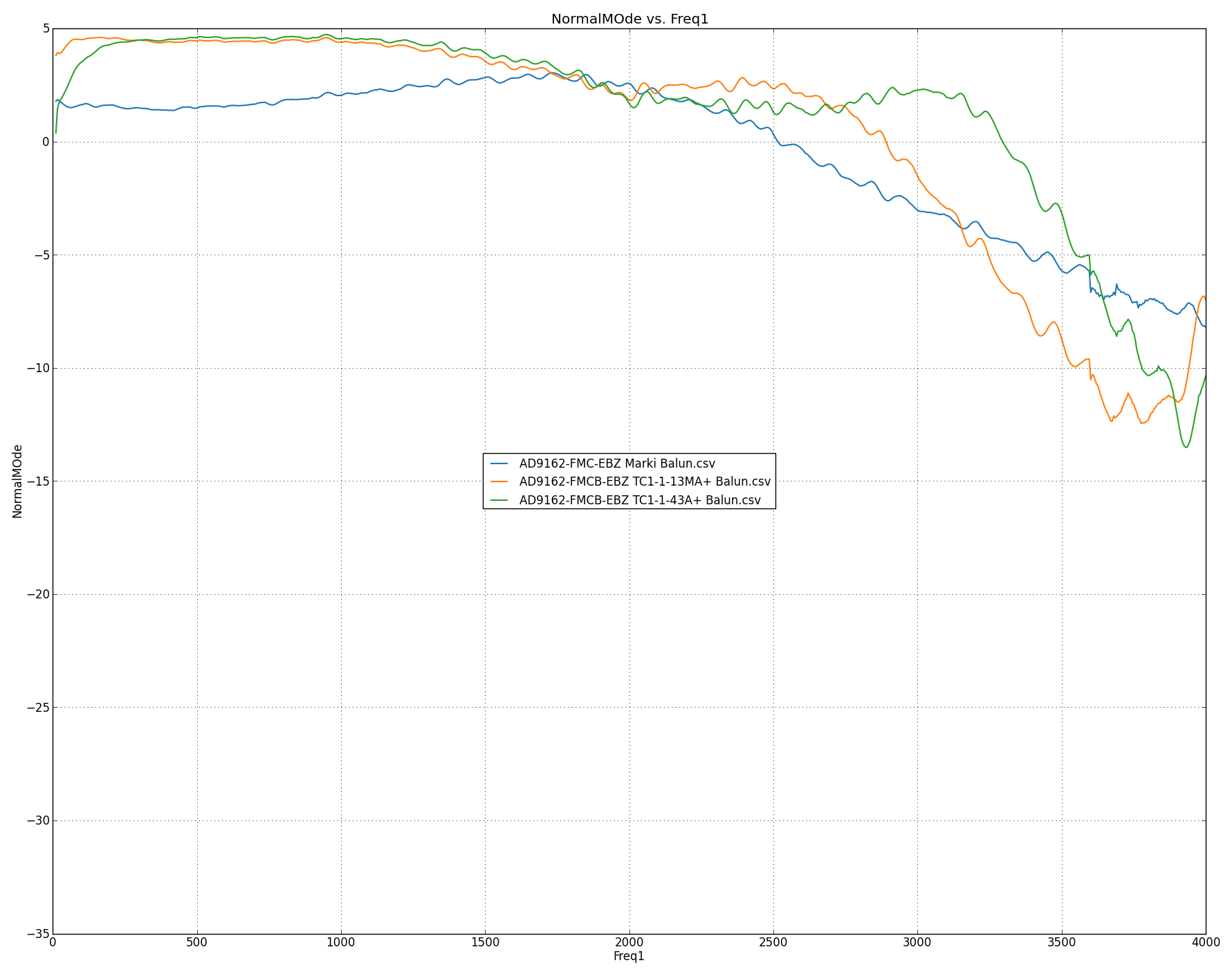 Figure 19. Typical fundamental amplitude responses of AD916x-FMCx-EBZ boards
The user can measure the ADF4355 performance by the SMA J62 as shown in Figure 2. The loop filter on the board is standard Type II, third order low pass filter. The user can customize and optimize the filter by using ADIsimPLL. https://form.analog.com/Form_Pages/RFComms/ADISimPll.aspx . The ADF4355 register settings generated by the AD916x Startup Wizard are typical. The user can use the standalone ADF4355 tools (http://www.analog.com/media/en/evaluation-boards-kits/evaluation-software/ADF4355_v0_53_3.zip) to regenerate new ADF4355 settings and enter them into the register map view of the ADF4355 by double-clicking into the Device View of the AD4355. The ADF4355 phase-frequency detector (PFD) spur level is related to the PFD frequency. A lower PFD frequency can help reduce the PFD spur, which also narrows the loop bandwidth and affects the PLL output phase noise. The PFD frequency used in the AD916x Startup Wizard is from 20MHz to 50MHz. The user can choose the PFD frequency according to the phase noise requirement and the PFD spur requirement.
There is a divide- by-4 divider (HMC362) on the board for providing the SERDES reference clock to the FPGA. The divider causes a ½ DAC clock rate spur to be shown on the ADF4355 output. i.e. there is a 2.5GHz spur on the ADF4355 output if the DAC clock rate is set to 5GHz. The spur level is around -55 dBc. The ½ DAC clock rate spur can mix with the DAC output to generate two new spurs (Fout+/- ½ CLK) if using the ADF4355 as clock source. The user may see these two additional spurs (Fout+/- ½ CLK ) at the DAC output. But these two spurs are not caused by the DAC. They disappear if an external clock is used instead. Figure 20 is one example to show the DAC spur differences between the on-board clock ADF4355 and an external clock. The spur in the red circle is at ½ FDAC-Fout.
 Figure 20. DAC output spur differences with different clock sources, ADF4355 and external clock SMA100
Due to the divide-by-4 circuit implemented on the eval board, several interpolation rates and lane counts related to the 3x interpolator are not supported on the evaluation board. These include 3x, 6 lanes and 6x, 3 lanes. The interpolation and lane count do not result in an integer divisible by 4, which is a requirement for the eval board. In the case of using 3 lanes or 6 lanes, the user must multiply the default vector length of 16384 by the lane number to ensure the DPG Downloader pattern is correctly sized. Otherwise, the pattern will not be correctly played from the pattern generator.
A comprehensive User’s Guide for the ACE software can be found on Analog Devices’ Wiki site here: http://wiki.analog.com/resources/tools-software/ace . A quick guide to the AD916x “plug-in” for ACE is given here. For any general information relating to the ACE tool itself, please consult the ACE user’s guide on the ADI Wiki. A picture of the ACE software screen is shown in Figure 21. In this view, the tabs for the ADS7+AD916x eval boards, the AD916x-FMCx-EBZ eval board, the AD916x device, and the AD916x Memory Map are shown near the red (1) in a circle, along with three tabs for each of the start-up scripts used in this User guide. The user can click on each tab to navigate to the various windows.
At the red (2) in a circle, the memory map view as registers or bit fields can be chosen. In Registers view, the full registers are shown, and in the area below the red (4), some registers have been expanded to show the bit field names and the detail that is possible to see. In the Bit Field view, the bit fields are listed alphabetically and have some “widgets” to control them and set bits, whereas in the Register view, the control is by bit or hex word. Both views can program the registers and it is merely user preference which is more convenient to use. At the red (3) is the Functional Group view. Because the AD916x has a large register map, the Functional Group view is useful to reduce the number of registers to view at a time. For example, Figure 21 shows the “JESD_Control” Functional Group, which is useful because the four needed registers to configure the JESD link are all in that group. By selecting this group and expanding the registers, the user can quickly find the registers and update their values. The “Apply Selected” or “Apply Changes” button, above the red (2), MUST be clicked after a register is changed to commit the change and program it to the device.
The Bit Fields view can be used in conjunction with Functional Groups. In that case, the Bit Fields associated with the selected Functional Group will be shown.
The red (5) is in the Macro Tools area, and is above the list of macros that are currently open in the session. The user can click the name of the desired macro to make it active in the screen. The “Play” button (right-pointing triangle) can be clicked and the selected macro played.
The red (6) is on the search field, which can be used to find a desired bit field.
 Figure 21. JESD_Control Functional Group view of AD916x in ACE
The Macro Tools window can be enabled by going to the “View” menu from the main menu bar and checking “Macro Tools”. JESD CONFIGURATION
The ADS7 is based on a Xilinx Virtex7 FPGA device. It is possible to configure another Xilinx Virtex7-based evaluation board to drive the AD916x EVB. Some items to note are given in this section to assist the customer in configuring the JESD204B transmitters. These can also be found in the AD916x data sheet rev PrE or later.
The JESD204B parameters for the AD916x-FMCx-EBZ EVB are given below.
Table 2. JESD Parameters for Interpolation Rate and Number of Lanes
| Interp | Lanes | M | F | S | PCLK period (DAC clocks) | LMFC period (DAC clocks) | Lane Rate @5GHz DACCLK |
|---|---|---|---|---|---|---|---|
| 1 | 8 | 1 | 1 | 4 | 16 | 128 | 12.5 |
| 2 | 6 | 2 | 2 | 3 | 12 | 192 | 16.66 (NOTE 1) |
| 2 | 8 | 2 | 1 | 2 | 16 | 128 | 12.5 |
| 3 | 6 | 2 | 2 | 3 | 18 | 288 | 11.11 |
| 3 | 8 | 2 | 1 | 2 | 24 | 192 | 8.33 |
| 4 | 3 | 2 | 4 | 3 | 12 | 384 | 16.66 (NOTE 1) |
| 4 | 4 | 2 | 1 | 1 | 16 | 128 | 12.5 |
| 4 | 6 | 2 | 2 | 3 | 24 | 384 | 8.33 |
| 4 | 8 | 2 | 1 | 2 | 32 | 256 | 6.25 |
| 6 | 3 | 2 | 4 | 3 | 18 | 576 | 11.11 |
| 6 | 4 | 2 | 1 | 1 | 24 | 192 | 8.33 |
| 6 | 6 | 2 | 2 | 3 | 36 | 576 | 5.55 |
| 6 | 8 | 2 | 1 | 2 | 48 | 384 | 4.16 |
| 8 | 2 | 2 | 2 | 1 | 16 | 256 | 12.5 |
| 8 | 3 | 2 | 4 | 3 | 24 | 768 | 8.33 |
| 8 | 4 | 2 | 1 | 1 | 32 | 256 | 6.25 |
| 8 | 6 | 2 | 2 | 3 | 48 | 768 | 4.16 |
| 8 | 8 | 2 | 1 | 2 | 64 | 512 | 3.12 |
| 12 | 2 | 2 | 2 | 1 | 24 | 384 | 8.33 |
| 12 | 3 | 2 | 4 | 3 | 36 | 1152 | 5.55 |
| 12 | 4 | 2 | 1 | 1 | 48 | 384 | 4.16 |
| 12 | 6 | 2 | 2 | 3 | 72 | 1152 | 2.77 |
| 12 | 8 | 2 | 1 | 2 | 96 | 768 | 2.08 |
| 16 | 1 | 2 | 4 | 1 | 16 | 512 | 12.5 |
| 16 | 2 | 2 | 2 | 1 | 32 | 512 | 6.25 |
| 16 | 3 | 2 | 4 | 3 | 48 | 1536 | 4.16 |
| 16 | 4 | 2 | 1 | 1 | 64 | 512 | 3.12 |
| 16 | 6 | 2 | 2 | 3 | 96 | 1536 | 2.08 |
| 16 | 8 | 2 | 1 | 2 | 128 | 1024 | 1.56 |
| 24 | 1 | 2 | 4 | 1 | 24 | 768 | 8.33 |
| 24 | 2 | 2 | 2 | 1 | 48 | 768 | 4.16 |
| 24 | 3 | 2 | 4 | 3 | 72 | 2304 | 2.77 |
| 24 | 4 | 2 | 1 | 1 | 96 | 768 | 2.08 |
| 24 | 6 | 2 | 2 | 3 | 144 | 2304 | 1.38 |
| 24 | 8 | 2 | 1 | 2 | 192 | 1536 | 1.04 |
NOTE 1: Maximum lane rate is 12.5 GHz, these modes must be run with the DAC rate below 3.75 GHz
Table 3. JESD parameters with fixed values
| Parameter | Value |
|---|---|
| K | 32 |
| N | 16 |
| NP | 16 |
| CF | 0 |
| HD | 1 |
| CS | 0 |
The physical lanes on the FMC connector are not necessarily connected to the same lanes on the AD916x. The AD916x does have a cross bar switch on the JESD204B link, but in the case of the ADS7 and AD916x, the switch is done using the crossbar in the Xilinx JESD Transmitter. Here is the mapping between the FMC lanes and the AD916x lanes on the AD916x-FMCx-EBZ evaluation board. The mapping to the Xilinx JESD204B IP is also given for reference. - Physical lane 0 on the FMC connector (DP0_C2M) is also lane 0 on AD916x (lane 0 out of the Xilinx JESD204 IP) - Physical lane 1 on the FMC connector (DP1_C2M) is also lane 1 on AD916x (lane 1 out of the Xilinx JESD204 IP) - Physical lane 2 on the FMC connector (DP2_C2M) is also lane 2 on AD916x (lane 2 out of the Xilinx JESD204 IP) - Physical lane 3 on the FMC connector (DP3_C2M) is also lane 3 on AD916x (lane 3 out of the Xilinx JESD204 IP) - Physical lane 4 on the FMC connector (DP4_C2M) is lane 5 on AD916x (lane 5 out of the Xilinx JESD204 IP) - Physical lane 5 on the FMC connector (DP5_C2M) is lane 7 on AD916x (lane 7 out of the Xilinx JESD204 IP) - Physical lane 6 on the FMC connector (DP6_C2M) is also lane 6 on AD916x (lane 6 out of the Xilinx JESD204 IP) - Physical lane 7 on the FMC connector (DP7_C2M) is lane 4 on AD916x (lane 4 out of the Xilinx JESD204 IP) There is also some P/N inversion between Tx and Rx on the AD916x-FMCx-EBZ EVB to ease lay out. They can easily be inverted in the Xilinx physical layer - Physical lanes 4-7 (DP4_C2M – DP7_C2M) on the FMC connector are inverted (P/N swapped) When getting the JESD link up and running, a few debug ideas are below. Watch the Sync lane - If Sync lane stays low, the 204B reference frequency needs to be adjusted - Sync lane toggles: P/N lanes needs to be adjusted (K character pass but not ILS with inverted polarity creating Sync toggling) - Sync stays high but not a good spectrum: Transport or mapping of lane is wrong
Record length shall be multiple of 3 in 3 lane/6lanes mode, otherwise the output spectrum isn’t correct. One example is shown in Figure 22.
There are five LEDs on the Eval board which are the 12v power supply LED, the ADF4355 locked LED, the USB connected LED, the AD916x PWR_BAD LED and the AD916x interruption LED. These LED are shown in Figure 23 . If the Eval board is configured correctly, 12v power LED, ADF4355 locked LED and USB connected LED shall be lit. PWR_BAD LED is lit when AD916x isn’t powered properly.
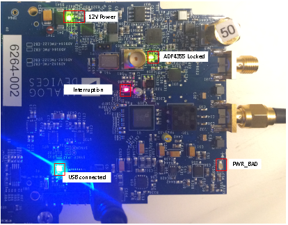 Figure 23. Five LEDs on the Eval Board
The AD916x-FMCx-EBZ eval board can be run with or without an ADS7. To download a valid image to the FPGA, open DPG Downloader with the USB cable connected to the PC and the ADS7. DPG Downloader will recognize the ADS7 and read the board ID of the AD916x-FMCx-EBZ (if it is connected) through the FMC connector. It will then download a valid image and power on the AD916x-FMCx-EBZ automatically.
There may be cases that one or the other software does not recognize the Eval boards. DPG Downloader can be open and a simple unplug-plug of the USB cable is normally sufficient. In the case of ACE, the ACE software will need to be closed, the USB cable plugged into the AD916x Eval board, power applied to the AD916x Eval board, and then ACE opened. This is an issue in ACE that will be addressed in a future release.
It can occur that the DPG Downloader software does not recognize the ADS7 board. Unplug the USB cable from the ADS7 and re-plug it in to the ADS7, and the DPG Downloader software should recognize the ADS7. If it does, it will download a Generic image to the FPGA. If the AD916x-FMCx-EBZ board is plugged into the ADS7 with the FMC connector prior to the USB cable being plugged into the ADS7, the DPG Downloader software should recognize the ADS7 and also read the AD916x-FMCx-EBZ identifier through the FMC connector, and download an AD916x image to the Eval board.
The start-up sequences referenced in this document have been tested in ADI’s lab on the AD916x-FMCx-EBZ evaluation board and are known working. There can be cases or situations when the JESD204B link does not come up. This section has several suggestions to debug the situation, but it is not an exhaustive list covering every possible scenario. When in doubt, power-cycle all hardware, re-open the ACE software, re-open the DPG Downloader software, and follow one of the Quick Start routines given in this guide. Then, notice the differences from the routines in this document as compared to the desired set-up, and carefully make the changes step-by-step and observe where the issue is created. Some debugging suggestions for times when the SERDES link does not come up: - If the SERDES PLL is locked (0x281[0]=1), then it may be necessary to reset the deframer by toggling bit 0x475[3] = 1, then 0. - If that doesn’t resolve the issue, it may be necessary to do a SERDES PLL re-calibration. To do this, set and reset 0x280[2], then do the de-framer reset toggle of 0x475[3] = 1, then 0.
If these don’t work, check to make sure the DPG Downloader has a pattern selected and the pattern is playing, i.e., sending data to the AD916x-FMCx-EBZ. The link will NOT come up if there is no data being sent to the DAC. Also, be sure to check that sub-class 0 is selected. This is the default sub-class and the User Guide examples all use sub-class 0. Finally, check that the JESD lane rate reported by DPG Downloader is what is expected based on the chosen JESD parameters.
If the board was previously configured for NCO mode, reset the board by doing a power cycle or writing 0x99 to register 0x000, then writing 0x18 to register 0x000. If the board was previously configured in a JESD mode, write the below sequence to disable the JESD204B interface: a. Reg 0x300 = 0x00 #Disable JESD204B links b. Reg 0x280 = 0x00 #Disable SERDES PLL This must be done before the SERDES configuration is changed. After disabling the JESD204B link, the below steps can be followed.
One of two possible errors can be generated, as shown in Figure 24 and Figure 25. Both of these indicate that the ACE software hasn’t recognized the AD916x-FMCx-EBZ. These can occur if the ACE software is started before powering up and connecting the AD916x-FMCx-EBZ Eval board to the PC, or if the Eval board is power-cycled and ACE is not re-started. This is a bug in ACE and will be corrected in a future release of ACE.
 Figure 24. Script error window indicating ACE does not recognize the AD916x-FMCx-EBZ eval board
 Figure 25. Register Write error indicating ACE does not recognize the AD916x-FMCx-EBZ Eval board
The most basic remedy for this issue is to close ACE and re-open it (re-start). As long as the AD916x-FMCx-EBZ is powered up and connected to the PC, ACE will recognize the Eval board and scripts and register writes will work again.
Check the board crystal, it can be 120MHz or 122.88MHz. The reference clock in the AD916x Startup Wizard should be set to the correct crystal frequency.
On a small number of pre-release eval boards, the ACE software selection for external clock does not actuate the RF switch to connect the external clock to the DAC clock input. A pre-release eval board will have a DAC on it with a package identifier as XBCZ or XBCAZ, as in AD9162XBCZ or AD9162XBCAZ. The root cause of this issue is a bug in the firmware loaded on the PIC microcontroller that is on the eval board. The firmware inadvertently omits control of the general purpose I/O (GPIO) line that controls the RF switch. Consequently, though the ACE software operates correctly, the switch does not actuate due to the firmware not controlling the GPIO line. If this issue is encountered, the board must be re-programmed with new firmware. Contact your local ADI sales person or distributor to arrange for this re-programming to be done.
The ADS7 firmware was updated at the factory prior to shipping. However, it is possible that a further update to the firmware was made after that time. If a firmware update is needed, a dialog stating that will be displayed and the user will not be able to use DPGDownloader until a firmware update is completed. To update the ADS7 firmware, open the DPG Downloader application and select the Advanced Debug button, as shown in Figure 26. Then, choose the “update” button. The updater should run and install the firmware update. It may be necessary to power cycle the ADS7 board, and to close and re-open DPG Downloader to recognize the update happened.