


This version is outdated by a newer approved version. This version (12 Jun 2022 15:39) is a draft.
Approvals: 0/1The Previously approved version (09 May 2018 17:22) is available.
This version (12 Jun 2022 15:39) is a draft.Approvals: 0/1The Previously approved version (09 May 2018 17:22) is available.
This is an old revision of the document!
Table of Contents
— Deferson Romero 10 Jun 2022 07:28
EVALUATING THE AD9121/AD9122 DIGITAL-TO-ANALOG CONVERTER
Preface
This user guide describes both the hardware and software setup needed to acquire data capture from AD9121-M5375-EBZ / AD9122-M5375-EBZ evaluation board to characterize AD9121 14-bit/AD9122 16-bit, Dual, 1.23GSPS, TxDAC+® digital-to-analog converter. This guide shows how AD9121-M5375-EBZ & AD9122-M5375-EBZ works with ADS7-V2/SDP-H1 controller board developed by Analog Devices. Link to the previous user guide document is provided for customers who still have the DPG2 controller board.
Typical Setup
 Figure 1a. AD9121-M5375-EBZ/AD9122-M5375-EBZ with SDP-H1 Setup
 Figure 1b. AD9121-M5375-EBZ/AD9122-M5375-EBZ with ADVS7-V2EBZ Setup
Tip: Click on any picture in this guide to open an enlarged version.
Helpful Files:
- AD9122 User Guide for DPG2 users
- IBIS Model: AD9122
- Bill of Materials: AD9122-M5372-EBZ REV A / AD9122-M5372-EBZ REV B / AD9122-M5375-EBZ REV E / AD9122-M5375-EBZ REV F
- PCB Gerber Files: AD9122-M5372-EBZ REV A / AD9122-M5372-EBZ REV B / AD9122-M5375-EBZ REV E / AD9122-M5375-EBZ REV F
- PCB Board Files: AD9122-M5372-EBZ REV A / AD9122-M5372-EBZ REV B / AD9122-M5375-EBZ REV E / AD9122-M5375-EBZ REV F
Software Needed:
- DPG Lite (installed with ACE)
Do not install ACE on a computer with DAC Software Suite.
Hardware Needed:
- AD9121-M5372-EBZ/AD9121-M5375-EBZ / AD9122-M5372-EBZ/AD9122-M5375-EBZ Evaluation Board
- SDP-H1 (EVAL-SDP-CH1Z) Evaluation Kit / ADS7-V2EBZ Evaluation Kit
- AD-DAC-FMC-ADP High-Speed DAC Evaluation Board to FMC Adaptor Board
- PC with ACE and DPG Lite Software Applications
- 5V Power Supply
- (2) Banana Plug Cables
- High-Frequency Continuous Wave Generator
- Signal/Spectrum Analyzer
- (2) SMA Cables
- The following are included in SDP-H1 Evaluation Kit:
- 12Vdc Wall Adapter
- USB-A to USB-Mini Cable
- The following are included in ADS7-V2 Evaluation Kit:
- 12Vdc Power Supply
- Power Cord
- USB-A to USB-B Cable
Quick Start Guide
Jumpers for Selecting the DAC Output
Jumpers JP4, JP5, JP6, and JP17 select the output configuration. By default, the DAC output connected to the LPF and the ADL537x analog quadrature modulator. The modulator LO input can be sourced through SMA connector J15 (LO_IN) with clock level at 3dBm. For selecting DAC output configuration, refer to Table 1 and Figure 2.
Table 1. Jumper Configurations for Viewing DAC Output and Modulator Output
| Output Viewed | Clock Input | SMA Output | Jumper Configuration |
|---|---|---|---|
| DAC Output | J1 | J3 (DAC1_P) or J8 (DAC1_P) | JP4 and JP5 center pads connected to outer pad, JP6 and JP7 center pads connected to outer pad |
| Modulator Output (Default) | J1 | J6 (MOD_OUT) | JP4 and JP5 center pads connected to inner pad, JP6 and JP7 center pads connected to inner pad |
 |  |
| DAC Output Configuration | Modulator Output Configuration |
Figure 2. AD9121-M5375-EBZ/AD9122-M5375-EBZ Output Configuration
Jumper for Selecting Power Supply
The evaluation board has a provision for on board or external power supply configuration. There are 7 pin jumpers on the evaluation board which shunted by default to use LDOs on board supply. The seventh pin jumper configures the voltage of the IOVDD supply. Refer to Table 2.
Table 2. Jumper Configurations for Power Supply
| Supply Rail | For LDO, Install Pin Jumper | For external Supply, Remove Pin Jumper and Use SMA |
|---|---|---|
| CVDD18 | JP2 | J4 |
| DVDD18 | JP3 | J11 |
| IOVDD | JP12 | J12 |
| AVDD33 | JP8 | J13 |
| XCVDD33 | JP9 | J10 |
| AVDD5 | JP11 | TP11(+5V), TP12 (GND) |
Evaluation Guide
- Make sure that on AD9121-M5375-EBZ/AD9122-M5375-EBZ, JP4, JP5, JP6, and JP17 are configured such that DAC output are connected with J3 (DAC1_P) or J8 (DAC2_P). Refer to Figure 2.
- Follow evaluation setup in Figure 1a and 1b.
- Attach the evaluation board to SDP-H1/ADS7-V2EBZ connector using the AD-DAC-FMC-ADP adapter board.
- Connect continuous wave generator for clock input to J1.
- Connect the DAC output from J3 (DAC1_P) or J8 (DAC2_P) to a signal/spectrum analyzer.
- Connect the evaluation board to PC via USB and to a 5V 1.5A power supply via banana plug cables.
- Connect SDP-H1/ADS7-V2EBZ to PC via USB and to a 12V 1A power supply.
- Set clock input to 500MHz and 2dBm.
- Open ACE. The board will automatically be recognized by the software. Otherwise, install the plugin for AD9121/AD9122 evaluation board. Double click this board then modify the configuration, as shown in Figure 3, and click “Apply”.
 Figure 3. ACE Initial Configuration Wizard when using SDP-H1/ADS7-V2EBZ
- Open the DPGDownloaderLite. The Evaluation Board AD9122/AD9122, Controller Board SDP-H1/ADS7-V2 and DCO Frequency of around 250MHz will be automatically detected by the DPG downloader.
- In DPGDownloaderLite, Add Generator Waveforms pulldown menu select Single Tone and apply the settings as shown in Figure 4. Set the Data Rate to 250MHz and Desired Frequency to 29 MHz. Set DAC Resolution to the DAC’s number of bits to: 14 bits for AD9121; 16 bits for AD9122. Check the “Generate Complex Data (I & Q)” box and “Unsigned Data” box.
- Select the in-phase tone from the I Data Vector pulldown menu and the quadrature tone from the Q Data Vector pulldown menu.
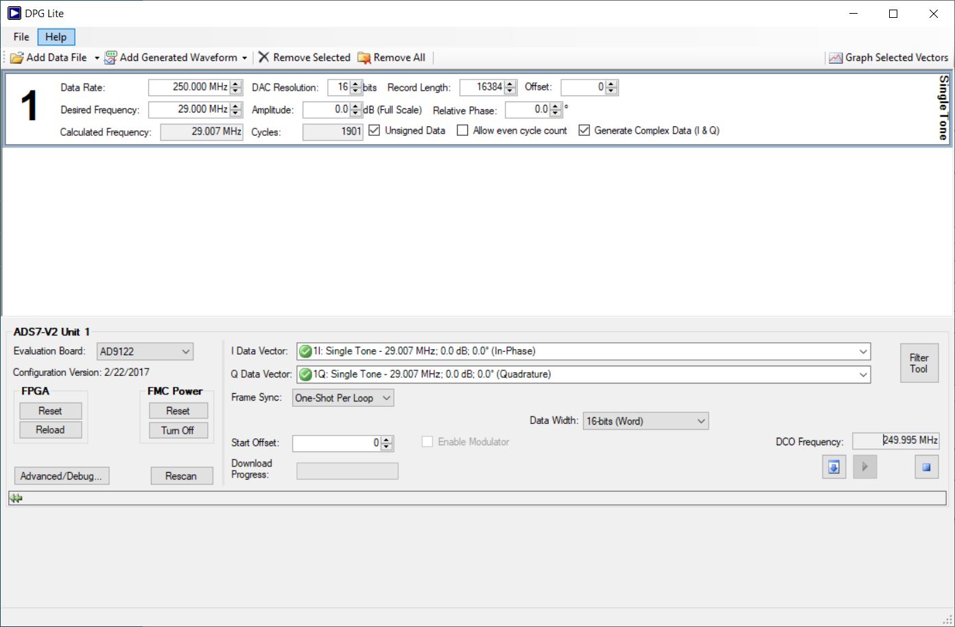 Figure 4. DPGDownloader Waveform Configuration for AD9122-M5375-EBZ
- Press the download arrow and then the play button. The spectrum similar to Figure 5 should appear in the signal/spectrum analyzer.
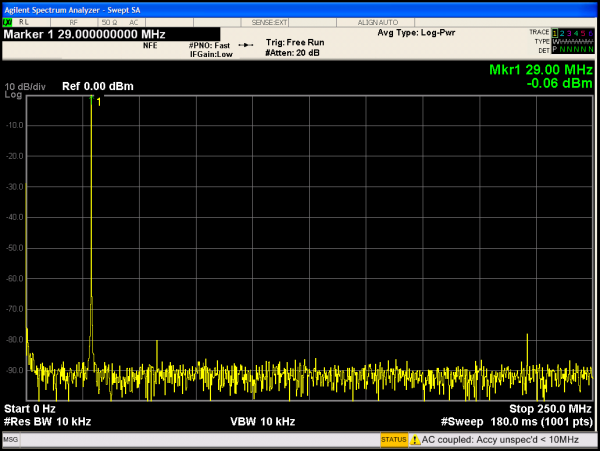 Figure 5. AD9122-M5375-EBZ FFT for Fdac=500MHz,2x Interpolation Fout=29MHz


resources/eval/dpg/ad9122-ebz.1655041148.txt.gz · Last modified: 12 Jun 2022 15:39 by Deferson Romero