EVALUATING THE AD9650 / AD9268 / AD9258 / AD9251 / AD9231 / AD9204 / AD9269 / AD9648 / AD9628 / AD9608 ANALOG-TO-DIGITAL CONVERTER
Preface
This user guide describes the evaluation boards, AD9650-105EBZ, AD9268-125EBZ, AD9258-125EBZ, AD9251-80EBZ, AD9231-80EBZ, AD9204-80EBZ, AD9269-80EBZ, AD9648-125EBZ, AD9628-125EBZ and AD9608-125EBZ that are used to evaluate the following Analog Devices, Inc., products: AD9650, AD9268, AD9258, AD9251, AD9231, AD9204, AD9269, AD9648, AD9628 and AD9608. These evaluation boards provide all of the support circuitry required to operate these parts in their various modes and configurations. The application software used to interface with the devices is also described.
The AD9650, AD9268, AD9258, AD9251, AD9231, AD9204, AD9269, AD9648, AD9628 and AD9608 data sheets provide additional information and should be consulted when using the evaluation board. All documents and software tools are available at www.analog.com/hsadcevalboard. For additional information or questions, send an email to highspeed.converters@analog.com.
The evaluation board covers multiple families of ADCs and is populated slightly differently between the families. Table 1 shows the four main families and the ADCs that fall within each family. When a reference is made to the AD9269, for example, this applies to all the ADCs within that family, that is, the AD9251, the AD9231, and the AD9204, and the AD9269.
Table 1. Family of Dual ADCs
| Family Name | ADCs within Each Family |
| AD9650 | AD9650 |
| AD9268 | AD9268, AD9258 |
| AD9269 | AD9251, AD9231, AD9204, AD9269 |
| AD9648 | AD9648, AD9628, AD9608 |
Typical Measurement Setup
Features
Helpful Documents
Software Needed
Design and Integration Files
Equipment Needed
Getting Started
Configuring the Board
Before using the software for testing, configure the evaluation board as follows:
Connect the evaluation board to the data capture board, as shown in Figure 1.
-
Connect one 6
V, 2.5 A switching power supply (such as the supplied CUI EPS060250UH-PHP-SZ supplied) to the
HSC-ADC-EVALCZ board.
Connect the
HSC-ADC-EVALCZ board to the PC with a
USB cable. (Connect to J6)
On the ADC evaluation board, confirm that three jumpers are installed on J302, one between Pin 1 and Pin 2, one between Pin 4 and Pin 5, and one between Pin 8 and Pin 9, to connect the
SPI bus to the DUT.
If using an AD9269 or AD9648 family board, ensure that J605 (OSC_EN) has a jumper installed to use the on-board 20
MHz/ 40
MHz/ 65
MHz/ 80
MHz Valpey Fisher VFAC3 oscillator. If using an AD9650 or AD9268 family board, make sure a low jitter sample clock is applied at J602 (see figure 2).
On the ADC evaluation board, use a clean signal generator with low phase noise to provide an input signal to the desired A and/or B channel(s). Use a 1
m, shielded, RG-58, 50 Ω coaxial cable to connect the signal generator: For best results, use a narrow-band, band-pass filter with 50 Ω terminations and an appropriate center frequency. (Analog Devices uses TTE, Allen Avionics, and
K & L band-pass filters.)
Evaluation Board Hardware
The evaluation board provides all of the support circuitry required to operate the AD9650, AD9268, AD9258, AD9251, AD9231, AD9204, AD9269, AD9648, AD9628 and AD9608 in their various modes and configurations. Figure 1 shows the typical bench characterization setup used to evaluate AC performance. It is critical that the signal sources used for the analog input and clock have very low phase noise (<1 ps rms jitter) to realize the optimum performance of the signal chain. Proper filtering of the analog input signal to remove harmonics and lower the integrated or broadband noise at the input is necessary to achieve the specified noise performance.
See the Getting Started section to get started, and Design and Integration Files sections for the complete schematics and layout diagrams. These diagrams demonstrate the routing and grounding techniques that should be applied at the system level when designing application boards using these converters.
Power Supplies
This evaluation board comes with a wall-mountable switching power supply that provides a 6 V, 2 A maximum output. Connect the supply to a 100 V ac to 240 V ac, 47 Hz to 63 Hz wall outlet. The output from the supply is provided through a 2.1 mm inner diameter jack that connects to the printed circuit board (PCB) at P101. The 6 V supply is fused and conditioned on the PCB before connecting to the low dropout linear regulators (default configuration) that supply the proper bias to each of the various sections on the board.
The evaluation board can be powered in a nondefault condition using external bench power supplies. To do this:
E101, E102, E114, E103, E105 and E107 ferrite beads can be removed to disconnect the outputs from the on-board LDOs.
Use P102 and P103 to connect a different supply for each section.
A 1.8
V supply is needed with 1A current capability for
DUT_AVDD and
DRVDD; however, it is recommended that separate supplies be used for both analog and digital domains.
An additional supply is also required to supply 1.8
V for digital support circuitry on the board,
DVDD. This should also have a 1 A current capability and can be combined with DRVDD with little or no degradation in performance.
To operate the evaluation board using the
SPI and alternate clock options, a separate 3.3
V analog supply is needed in addition to the other supplies. This 3.3
V supply, or
3V_CLK, should have a 1 A current capability.
Two additional supplies, 5V_AMPVDD and 3V_AMPVDD, are used to bias the optional input path amplifiers and optional VREF buffer. If used, these supplies should each have 1 A current capability.
A second optional power supply configuration allows replacing the LDOs that supply the AVDD and DRVDD rails of the ADC with the dual switching power supply ADP2114 step-down dc-to-dc regulator. To configure the board to operate from the ADP2114, the following changes must be incorporated. (See Design and Integration Files for specific recommendations for part values):
Install R120 and R122 to enable the ADP2114. Also, R107, R109, R110, R111, C108, C109, R108, R118, C110, C111, C112, C113, R116, R117, C137, C140, L101, L102, E116, E117, R124, R125, R126, R127, JP102, JP104, E104, E106, and E108.
Remove JP101, JP103, E103, E105 and E107.
Making these changes enables the switching converter to power the ADC. Using the switching converters as the ADC power source is more efficient than using the default LDOs.
When connecting the ADC clock and analog source, use clean signal generators with low phase noise, such as the Rohde & Schwarz SMA, or HP 8644B signal generators or an equivalent. Use a 1 m shielded, RG-58, 50 Ω coaxial cable for connecting to the evaluation board. Enter the desired frequency and amplitude in the signal generators (see the Specifications section in the data sheet of the respective part). When connecting the analog input source, use of a multipole, narrow-band band-pass filter with 50 Ω terminations is recommended. Analog Devices, Inc., uses band-pass filters from TTE, Allen Avionics and K & L Microwave, Inc. Connect the filters directly to the evaluation board.
If an external clock source is used, it should also be supplied with a clean signal generator as previously specified. Analog Devices evaluation boards typically can accept ~2.8 V p-p or 13 dBm sine wave input for the clock.
Output Signals
The default setup uses the Analog Devices high speed converter evaluation platform (HSC-ADC-EVALCZ) for data capture. The CMOS output signals from Channel A and Channel B are buffered through U801 and U802 and are routed through P903 and P902, respectively, to the FPGA on the data capture board. For more information on the data capture board and its optional settings, visit www.analog.com/hsadcevalboard.
Default Operation and Jumper Selection Settings
This section explains the default and optional settings or modes allowed on the AD9650, AD9268, AD9258, AD9251, AD9231, AD9204, AD9269, AD9648, AD9628 and AD9608.
Summary of Jumper Settings
Table 2.1. Jumper Configuration for AD9650.
| Jumper | Description |
| J201 | Pin 4 and Pin 6 - Default VREF configuration, SENSE pin is connected to AGND for internal VREF operation of 1.35 V for a 2.7 V p-p full-scale range.
Pin 4 and Pin 2 - SENSE pin is connected to AVDD pin for external VREF operation. |
| J605 | No Jumper - Default operation using external clock.
With jumper - Enable the on-board oscillator (Add 0 Ω resistor at C610, remove R602). |
| J205 | Pin 1 and Pin 2 - Enable the Power-Down feature, PDWN pin to DRVDD.
Pin 3 and Pin 4 - Disable the outputs using the /OE pin, /OE pin to DRVDD |
| J302 | Pin 1 and Pin 2, Pin 4 and Pin 5, Pin 8 and Pin 9 - Default configuration.
Pin 2 and Pin 3 - Enable the DCS.
Pin 5 and Pin 6 - Data format set to twos complement.
No Jumper - Non-SPI mode, operate the DUT without SPI. DCS is disable, data format is set to offset binary. |
Table 2.2. Jumper Configuration for AD9268 and AD9258.
| Jumper | Description |
| J201 | Pin 4 and Pin 6 - Default VREF configuration, SENSE pin is connected to AGND for internal VREF operation of 1.0 V for a 2.0 V p-p full-scale range.
Pin 4 and Pin 3 - SENSE pin is connected to VREF pin for internal VREF operation of 0.5 V for a 1.0 V p-p full-scale range. (See VREF for more info.)
Pin 4 and Pin 2 - SENSE pin is connected to AVDD pin for external VREF operation.
No jumper - Programmable reference mode, using resistor divider at R204 and R205.\\ |
| J605 | No Jumper - Default operation using external clock.
With jumper - Enable the on-board oscillator (Add 0 Ω resistor at C610, remove R602). |
| J205 | Pin 1 and Pin 2 - Enable the Power-Down feature, PDWN pin to DRVDD.
Pin 3 and Pin 4 - Disable the outputs using the /OE pin, /OE pin to DRVDD |
| J302 | Pin 1 and Pin 2, Pin 4 and Pin 5, Pin 8 and Pin 9 - Default configuration.
Pin 2 and Pin 3 - Enable the DCS.
Pin 5 and Pin 6 - Data format set to twos complement.
No Jumper - Non-SPI mode, operate the DUT without SPI. DCS is disable, data format is set to offset binary. |
Table 2.3. Jumper Configuration for AD9269, AD9251, AD9231, AD9204, AD9648, AD9628 and AD9608.
| Jumper | Description |
| J201 | Pin 4 and Pin 6 - Default VREF configuration, SENSE pin is connected to AGND for internal VREF operation of 1.0 V for a 2.0 V p-p full-scale range.
Pin 4 and Pin 2 - SENSE pin is connected to AVDD pin for external VREF operation of 1.0 V for a 2.0 V p-p full-scale range. |
| J605 | With jumper - Default configuration, used the on-board oscillator.
No Jumper - Use external clock. |
| J205 | Pin 1 and Pin 2 - Enable the Power-Down feature, PDWN pin to DRVDD.
Pin 3 and Pin 4 - Disable the outputs using the /OE pin, /OE pin to DRVDD |
| J302 | Pin 1 and Pin 2, Pin 4 and Pin 5, Pin 8 and Pin 9 - Default configuration.
Pin 2 and Pin 3 - Enable the DCS.
Pin 5 and Pin 6 - Data format set to twos complement.
No Jumper - Non-SPI mode, operate the DUT without SPI. DCS is disable, data format is set to offset binary. |
The A and B channel inputs on the evaluation board are set up for a double balun-coupled analog input with a 50 Ω impedance.
The default input network, as configured on the AD9650 evaluation board, is shown in Figure 3.1

Figure 3.1 Default Analog Input Configuration of the AD9650 Family
For the AD9268 family, the default analog input configuration supports analog input frequencies of up to ~250 MHz (see Figure 3.2). The input network is optimized to support a wide frequency band. See the AD9258 and AD9268 data sheets for additional information on the recommended networks for different input frequency ranges.

Figure 3.2. Default Analog Input Configuration of the AD9268 Family
For the AD9269 and AD9648 family, the default analog input configuration supports analog input frequencies of up to ~150 MHz (see Figure 3.3 & 3.4). The nominal input drive level is 10dBm to achieve 2 V p-p full scale into 50 Ω. At higher frequencies, slightly higher input drive levels are required due to losses in the front-end network.

Figure 3.3. Default Analog Input Configuration of the AD9269 Family

Figure 3.4. Default Analog Input Configuration of the AD9648 Family
Optionally, the Channel A input on the board can be configured to use the AD8375 digitally variable gain amplifier (DVGA). The AD8375 component is included on the evaluation board at U401. However, the path into and out of the AD8375 can be configured in many different ways depending on the application; therefore, the parts in the input and output path are left unpopulated. Users should see the AD8375 data sheet for additional information on the part and for configuring the inputs and outputs. The AD8375 by default is held in power-down mode but can be enabled by adding a jumper on J403.
The Channel B input is also set up with an optional input path through the ADL5562 ultralow distortion RF/IF differential amplifier. Similar to Channel A, the amplifier is included on the board at U501; however, the input-/output-related components are not included. Users should see the ADL5562 data sheet for additional information on this part and for configuring the inputs and outputs. The ADL5562 is also normally held in power-down mode and can be enabled by adding a jumper on J503. The ADL5562 on the Channel B input can also be substituted with ADA4937 or the ADA4938 to allow evaluation of these parts with the ADC.
VREF
The default VREF configuration is to connect the SENSE pin to AGND for internal VREF operation. This is done by connecting Pin 4 and Pin 6 on Header J201. Table 2 summarizes the internal VREF voltage for the different families of ADCs.
Table 3. Default VREF Configuration
The AD9650, AD9269 and AD9648 families operate with a fixed reference.
For the AD9268 family, the reference voltage can be changed to 0.5 V for a 1.0 V p-p full-scale range by moving the SENSE pin jumper connection on J201 to Pin 4 and Pin 3.
To use the programmable reference mode for the AD9268 family, a resistor divider can be set up by installing R204 and R205. The jumper on J201 should be removed for this mode of operation. See the data sheet of the specific part for the additional information on using the programmable reference mode.
A separate unpopulated external reference option using the AD1580 reference and the AD822 amplifier is also included on the evaluation board. To enable the external reference, populate CR201, U202, R202, R201, C201 and C202 with the values shown in the Evaluation Board Schematics at Design and Integration Files. The J201 jumper should be placed between Pin 4 and Pin 2 to set the reference input to the external reference mode.
RBIAS
RBIAS has a default setting of 10 kΩ (R206) to ground and is used to set the ADC core bias current. Note that using a resistor value other than a 10 kΩ, 1% resistor for RBIAS may degrade the performance of the device.
Clock Circuitry
The default clock input circuit on the AD9269 and AD9648 evaluation board family uses a simple transformer-coupled circuit using a high bandwidth 1:1 impedance ratio transformer (T601) that adds a low amount of jitter to the clock path. The clock input is 50 Ω terminated and ac-coupled to handle single-ended sine wave types of inputs. The transformer converts the single-ended input to a differential signal that is clipped by CR601 before entering the ADC clock inputs.
The board is set by default to be clocked through the transformer-coupled input network from the crystal oscillator, Y601. This oscillator is a low phase noise oscillator from Valpey Fisher (AD9269: VFAC3-BHL-20MHz/ VFAC3-BHL-40MHz/ VFAC3-BHL-65MHz/ VFAC3-BHL-80MHz & AD9648: VFAC3-BHL-105MHz/ VFAC3-BHL-125MHz). If a different clock source is desired, remove J605 to disable the oscillator from running and connect the external clock source to the SMA connector, J602 (labeled ENCODE+).
The default clock input circuitry on the AD9650 and AD9268 family evaluation boards uses a similar circuit to the AD9269 family but uses a higher bandwidth 1:1 impedance ratio balun (T602) that adds a low amount of jitter to the clock path. The clock input is again 50Ω terminated and ac-coupled to handle single-ended sine wave types of inputs. The balun converts the single-ended input to a differential signal that is clipped before entering the ADC clock inputs.
The board is set by default to use an external clock generator. An external clock source capable of driving a 50 Ω terminated input should be connected to J602. This family is shipped from Valpey Fisher with a low phase noise oscillator installed. The oscillator frequency is set to match the rated speed of the part: 125 MHz, 105 MHz, or 80 MHz for the AD9268 family and 105 MHz, 80 MHz, 65 MHz, or 25 MHz, for the AD9650 family. To enable the oscillator, install J605, and to connect it into the clock path, add a 0 Ω resistor at C610. R602 should also be removed to remove the 50 Ω termination from the output of the oscillator.
A differential LVPECL clock driver output can also be used to clock the ADC input using to AD9517 (U701). To place the AD9517 into the clock path, populate R607 and R608 with 0 Ω resistors and remove R609 and R610 to disconnect the default clock path inputs. In addition, populate R731 and R732 with 0 Ω resistors and remove R611 and R612 to disconnect the default clock path outputs and insert the AD9517 LVPECL Output 3. The AD9517 must be configured through SPI controller software to set up the PLL and other operation modes. Consult the AD9517 data sheet for more information about these and other options.
Non-SPI Mode
For users who want to operate the DUT without using SPI, remove the shorting jumpers on J302. This disconnects the CSB/CS, SCLK/DFS and SDIO/DCS pins from the SPI control bus, allowing the DUT to operate in non-SPI mode. In this mode the SDIO/DCS pin controls the duty cycle stabilizer, and the SCLK/DFS pin controls the digital output format. Table 2 and Table 3 specify the settings for pin mode operation.
Table 4. Duty Cycle Stabilizer Settings
| SDIO (J302 Pin 2) | DCS Mode |
| AVDD (J302 Pin 2 to Pin 3) | DCS Enable |
| AGND (“float” J302 Pin 2) | DCS Disable |
Table 5. Digital Test Pattern Pin Settings
| SCLK (J302 Pin 5) | Output Format |
| AVDD (J302 Pin 5 to Pin 6) | Twos Complement |
| AGND (“float” J302 Pin 5) | Offset Binary |
Note that the above settings only apply when CSB is tied high (J302 Pin 8 “floating”) at power up.
Additional information on the Standalone (PIN) Mode is provided in the data sheet.
Using The Software for Testing
Setting up the ADC Data Capture (Visual Analog Software)
After configuring the board, set up the ADC data capture using the following steps:
Open VisualAnalog on the connected PC. The appropriate part type should be listed in the status bar of the
VisualAnalog – New Canvas window. Select the template that corresponds to the type of testing to be performed (see Figure 4, where the
AD9268 is shown as example but select
AD9650).

Figure 4. VisualAnalog, New Canvas Window
After the template is selected, a message appears asking if the default configuration can be used to program the FPGA (Figure 5). Click
YES and the window closes.

Figure 5. VisualAnalog Default Configuration Message
To change features to settings other than the default settings, click the
Expand Display button, located on the bottom right corner of the window, to see what is shown in Figure 7. Detailed instructions for changing the features and capture settings can be found in the
AN-905 Application Note,
VisualAnalog Converter Evaluation Tool Version 1.0 User Manual. After the changes are made to the capture settings, click the
Collapse Display button (see Figure 6).

Figure 6. VisualAnalog Window Toolbar, Collapsed Display

Figure 7. VisualAnalog, Main Window Expanded Display
Setting up the SPI Controller Software
After the ADC data capture board setup is complete, set up the SPI controller software using the following procedure:
Open the
SPI controller software by going to the
Start menu or by double-clicking the
SPIController software desktop icon. If prompted for a configuration file, select the appropriate one. If not, check the title bar of the window to determine which configuration is loaded. If necessary, choose
Cfg Open from the
File menu and select the appropriate file based on your part type. Note that the
CHIP ID(1) box should be filled to indicate whether the correct
SPI controller configuration file is loaded (see Figure 8).

Figure 8. SPI Controller, CHIP ID(1) Box
Click the
New DUT button in the
SPIController window or
Reset at
CHIP PORT CFG(0) to reinitializes the DUT interface (see Figure 9).

Figure 9. SPI Controller, New DUT Button
In the
ADCBase 0 tab of the
SPIController window, find the
CLOCK DIVIDE(B) box. If using the clock divider, use the drop-down box to select the correct clock divide ratio, if necessary. Also, check if the
VREF(18) box is set to
2.70Vp-p (see Figure 10). See the appropriate part data sheet, the
AN-878 Application Note,
High Speed ADC SPI Control Software, and the
AN-877 Application Note,
Interfacing to High Speed ADCs via SPI, for additional information on the available settings.

Figure 10. SPI Controller, ADCBase0 Tab
Note that other settings can be changed on the
ADCBase 0 page (see Figure 10) and the
ADC A and
ADC B pages (see Figure 11) to set up the part in the desired mode. The
ADCBase 0 page settings affect the entire part, whereas the settings on the
ADC A and
ADC B pages affect the selected channel only. See the appropriate part data sheet; the
AN-878 Application Note,
High Speed ADC SPI Control Software, and the
AN-877 Application Note,
Interfacing to High Speed ADCs via SPI, for additional information on the available settings.

Figure 11. SPI Controller, Example ADC A Tab
Click the
Run button in the
VisualAnalog toolbar (see Figure 12).

Figure 12. Run Button (Encircled in Red) in VisualAnalog Toolbar, Collapsed Display
Adjusting the Amplitude of the Input Signal
The next step is to adjust the amplitude of the input signal for each channel as follows:
Adjust the amplitude of the input signal so that the fundamental is at -1.0
dBFS. Examine the
Fund Power reading in the left panel of the
VisualAnalog Graph - AD9650 Average FFT window (see Figure 13) to verify this.

Figure 13. Graph Window of VisualAnalog
Repeat this procedure for Channel B.
Click the disk icon within the
Graph window to save the performance plot data as
.csv formatted file. See Figure 14 for
AD9650 example. Please refer to the respective data sheet of the product of interest for its typical FFT performance.
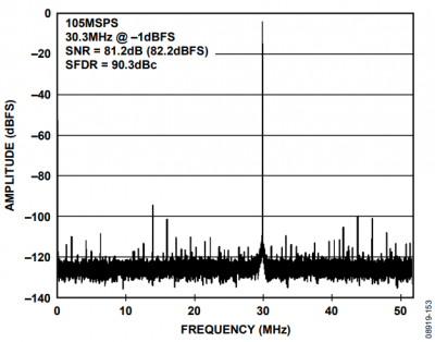
Figure 14. Typical FFT, AD9650
Setting up the ADC Data Capture (Visual Analog Software)
After configuring the board, set up the ADC data capture using the following steps:
Open VisualAnalog on the connected PC. The appropriate part type should be listed in the status bar of the
VisualAnalog – New Canvas window. Select the template that corresponds to the type of testing to be performed (see Figure 4, where the
AD9268 is shown as example).

Figure 4. VisualAnalog, New Canvas Window
After the template is selected, a message appears asking if the default configuration can be used to program the FPGA (Figure 5). Click
YES and the window closes.

Figure 5. VisualAnalog Default Configuration Message
To change features to settings other than the default settings, click the
Expand Display button, located on the bottom right corner of the window, to see what is shown in Figure 7. Detailed instructions for changing the features and capture settings can be found in the
AN-905 Application Note,
VisualAnalog Converter Evaluation Tool Version 1.0 User Manual. After the changes are made to the capture settings, click the
Collapse Display button (see Figure 6).

Figure 6. VisualAnalog Window Toolbar, Collapsed Display

Figure 7. VisualAnalog, Main Window Expanded Display
Setting up the SPI Controller Software
After the ADC data capture board setup is complete, set up the SPI controller software using the following procedure:
Open the
SPI controller software by going to the
Start menu or by double-clicking the
SPIController software desktop icon. If prompted for a configuration file, select the appropriate one. If not, check the title bar of the window to determine which configuration is loaded. If necessary, choose
Cfg Open from the
File menu and select the appropriate file based on your part type. Note that the
CHIP ID(1) box should be filled to indicate whether the correct
SPI controller configuration file is loaded (see Figure 8).

Figure 8. SPI Controller, CHIP ID(1) Box
Click the
New DUT button in the
SPIController window or
Reset at
CHIP PORT CFG(0) to reinitializes the DUT interface (see Figure 9).

Figure 9. SPI Controller, New DUT Button
In the
ADCBase 0 tab of the
SPIController window, find the
CLOCK DIVIDE(B) box. If using the clock divider, use the drop-down box to select the correct clock divide ratio, if necessary. Also, check if the
VREF(18) box is set to
2.00Vp-p (see Figure 10). See the appropriate part data sheet, the
AN-878 Application Note,
High Speed ADC SPI Control Software, and the
AN-877 Application Note,
Interfacing to High Speed ADCs via SPI, for additional information on the available settings.

Figure 10. SPI Controller, ADCBase0 Tab
Note that other settings can be changed on the
ADCBase 0 page (see Figure 10) and the
ADC A and
ADC B pages (see Figure 11) to set up the part in the desired mode. The
ADCBase 0 page settings affect the entire part, whereas the settings on the
ADC A and
ADC B pages affect the selected channel only. See the appropriate part data sheet; the
AN-878 Application Note,
High Speed ADC SPI Control Software, and the
AN-877 Application Note,
Interfacing to High Speed ADCs via SPI, for additional information on the available settings.

Figure 11. SPI Controller, Example ADC A Tab
Click the
Run button in the
VisualAnalog toolbar (see Figure 12).

Figure 12. Run Button (Encircled in Red) in VisualAnalog Toolbar, Collapsed Display
Adjusting the Amplitude of the Input Signal
The next step is to adjust the amplitude of the input signal for each channel as follows:
Adjust the amplitude of the input signal so that the fundamental is at -1.0
dBFS. Examine the
Fund Power reading in the left panel of the
VisualAnalog Graph - AD9268 Average FFT window (see Figure 13) to verify this.

Figure 13. Graph Window of VisualAnalog
Repeat this procedure for Channel B.
Click the disk icon within the
Graph window to save the performance plot data as
.csv formatted file. See Figure 14 for
AD9268 example. Please refer to the respective data sheet of the product of interest for its typical FFT performance.

Figure 14. Typical FFT, AD9268
Setting up the ADC Data Capture (Visual Analog Software)
After configuring the board, set up the ADC data capture using the following steps:
Open VisualAnalog on the connected PC. The appropriate part type should be listed in the status bar of the
VisualAnalog – New Canvas window. Select the template that corresponds to the type of testing to be performed (see Figure 4, where the
AD9269 is shown as example).

Figure 4. VisualAnalog, New Canvas Window
After the template is selected, a message appears asking if the default configuration can be used to program the FPGA (Figure 5). Click
YES and the window closes.

Figure 5. VisualAnalog Default Configuration Message
To change features to settings other than the default settings, click the
Expand Display button, located on the bottom right corner of the window, to see what is shown in Figure 7. Detailed instructions for changing the features and capture settings can be found in the
AN-905 Application Note,
VisualAnalog Converter Evaluation Tool Version 1.0 User Manual. After the changes are made to the capture settings, click the
Collapse Display button (see Figure 6).

Figure 6. VisualAnalog Window Toolbar, Collapsed Display

Figure 7. VisualAnalog, Main Window Expanded Display
Setting up the SPI Controller Software
After the ADC data capture board setup is complete, set up the SPI controller software using the following procedure:
Open the
SPI controller software by going to the
Start menu or by double-clicking the
SPIController software desktop icon. If prompted for a configuration file, select the appropriate one. If not, check the title bar of the window to determine which configuration is loaded. If necessary, choose
Cfg Open from the
File menu and select the appropriate file based on your part type. Note that the
CHIP ID(1) box should be filled to indicate whether the correct
SPI controller configuration file is loaded (see Figure 8).

Figure 8. SPI Controller, CHIP ID(1) Box
Click the
New DUT button in the
SPIController window or
Reset at
CHIP PORT CFG(0) to reinitializes the DUT interface (see Figure 9).

Figure 9. SPI Controller, New DUT Button
In the
ADCBase 0 tab of the
SPIController window, find the
CLOCK DIVIDE(B) box. If using the clock divider, use the drop-down box to select the correct clock divide ratio, if necessary. See the appropriate part data sheet, the
AN-878 Application Note,
High Speed ADC SPI Control Software, and the
AN-877 Application Note,
Interfacing to High Speed ADCs via SPI, for additional information on the available settings.

Figure 10. SPI Controller, ADCBase 0 Tab
Note that other settings can be changed on the
ADCBase 1 page (see Figure 11) and the
ADC A and
ADC B pages (see Figure 12 and 13) to set up the part in the desired mode. The
ADCBase 0 and
ADCBase 1 page settings affect the entire part, whereas the settings on the
ADC A and
ADC B pages affect the selected channel only. See the appropriate part data sheet; the
AN-878 Application Note,
High Speed ADC SPI Control Software, and the
AN-877 Application Note,
Interfacing to High Speed ADCs via SPI, for additional information on the available settings.

Figure 11. SPI Controller, ADCBase 1 Tab
In
ADC A tab click
ADC 0 on
OUTPUT ASSIGN(2E) and in
ADC B tab click
ADC 1 on
OUTPUT ASSIGN(2E) to refresh the registers.

Figure 12. SPI Controller, ADC A Tab

Figure 13. SPI Controller, ADC B Tab
Click the
Run button in the
VisualAnalog toolbar (see Figure 14).

Figure 14. Run Button (Encircled in Red) in VisualAnalog Toolbar, Collapsed Display
Adjusting the Amplitude of the Input Signal
The next step is to adjust the amplitude of the input signal for each channel as follows:
Adjust the amplitude of the input signal so that the fundamental is at -1.0
dBFS. Examine the
Fund Power reading in the left panel of the
VisualAnalog Graph - AD9269 Average FFT window (see Figure 15) to verify this.

Figure 15. Graph Window of VisualAnalog
Repeat this procedure for Channel B.
Click the disk icon within the
Graph window to save the performance plot data as
.csv formatted file. See Figure 16 for
AD9269 example. Please refer to the respective data sheet of the product of interest for its typical FFT performance.

Figure 16. Typical FFT, AD9269
Setting up the ADC Data Capture (Visual Analog Software)
After configuring the board, set up the ADC data capture using the following steps:
Open VisualAnalog on the connected PC. The appropriate part type should be listed in the status bar of the
VisualAnalog – New Canvas window. Select the template that corresponds to the type of testing to be performed (see Figure 4, where the
AD9269 is shown as example).
Figure 4. VisualAnalog, New Canvas Window
After the template is selected, a message appears asking if the default configuration can be used to program the FPGA (Figure 5). Click
YES and the window closes.
Figure 5. VisualAnalog Default Configuration Message
To change features to settings other than the default settings, click the
Expand Display button, located on the bottom right corner of the window, to see what is shown in Figure 7. Detailed instructions for changing the features and capture settings can be found in the
AN-905 Application Note,
VisualAnalog Converter Evaluation Tool Version 1.0 User Manual. After the changes are made to the capture settings, click the
Collapse Display button (see Figure 6).
Figure 6. VisualAnalog Window Toolbar, Collapsed Display
Figure 7. VisualAnalog, Main Window Expanded Display
Setting up the SPI Controller Software
After the ADC data capture board setup is complete, set up the SPI controller software using the following procedure:
Open the
SPI controller software by going to the
Start menu or by double-clicking the
SPIController software desktop icon. If prompted for a configuration file, select the appropriate one. If not, check the title bar of the window to determine which configuration is loaded. If necessary, choose
Cfg Open from the
File menu and select the appropriate file based on your part type. Note that the
CHIP ID(1) box should be filled to indicate whether the correct
SPI controller configuration file is loaded (see Figure 8).
Figure 8. SPI Controller, CHIP ID(1) Box
Click the
New DUT button in the
SPIController window or
Reset at
CHIP PORT CFG(0) to reinitializes the DUT interface (see Figure 9).
Figure 9. SPI Controller, New DUT Button
In the
ADCBase 0 tab of the
SPIController window, find the
CLOCK DIVIDE(B) box. If using the clock divider, use the drop-down box to select the correct clock divide ratio, if necessary. See the appropriate part data sheet, the
AN-878 Application Note,
High Speed ADC SPI Control Software, and the
AN-877 Application Note,
Interfacing to High Speed ADCs via SPI, for additional information on the available settings.
Figure 10. SPI Controller, ADCBase 0 Tab
Note that other settings can be changed on the
ADCBase 1 page (see Figure 11) and the
ADC A and
ADC B pages (see Figure 12 and 13) to set up the part in the desired mode. The
ADCBase 0 and
ADCBase 1 page settings affect the entire part, whereas the settings on the
ADC A and
ADC B pages affect the selected channel only. See the appropriate part data sheet; the
AN-878 Application Note,
High Speed ADC SPI Control Software, and the
AN-877 Application Note,
Interfacing to High Speed ADCs via SPI, for additional information on the available settings.
Figure 11. SPI Controller, ADCBase 1 Tab
In
ADC A tab click
ADC 0 on
OUTPUT ASSIGN(2E) and in
ADC B tab click
ADC 1 on
OUTPUT ASSIGN(2E) to refresh the registers.
Figure 12. SPI Controller, ADC A Tab
Figure 13. SPI Controller, ADC B Tab
Click the
Run button in the
VisualAnalog toolbar (see Figure 14).
Figure 14. Run Button (Encircled in Red) in VisualAnalog Toolbar, Collapsed Display
Adjusting the Amplitude of the Input Signal
The next step is to adjust the amplitude of the input signal for each channel as follows:
Adjust the amplitude of the input signal so that the fundamental is at -1.0
dBFS. Examine the
Fund Power reading in the left panel of the
VisualAnalog Graph - AD9269 Average FFT window (see Figure 15) to verify this.
Figure 15. Graph Window of VisualAnalog
Repeat this procedure for Channel B.
Click the disk icon within the
Graph window to save the performance plot data as
.csv formatted file. See Figure 16 for
AD9269 example. Please refer to the respective data sheet of the product of interest for its typical FFT performance.
Figure 16. Typical FFT, AD9269
Troubleshooting Tips
If the FFT plot appears abnormal, do the following:
If you see a normal noise floor when you disconnect the signal generator from the analog input, be sure you are not overdriving the ADC. Reduce the input level, if necessary.
If you see an abnormal noise floor, go to the ADCBase0 tab of the SPIController window and toggle the Chip Power Mode in MODES(8) from Chip Run to Reset and back.
In VisualAnalog, click the Settings button in the Input Formatter block. Check that Number Format is set to correct encoding (offset binary by default). Also, check that it matches the data format selected in the SPIController → ADCBase0 → OUTPUT MODE(14). Repeat for the other channel.
If the FFT appears normal but the performance is poor, check the following:
Make sure that an appropriate filter is used on the analog input.
Make sure that the signal generators for the clock and the analog input are clean (low phase noise).
Change the analog input frequency slightly if noncoherent sampling is being used.
Make sure that the
SPI configuration file matches the product being evaluated.
If the FFT window remains blank after Run is clicked, do the following:
Make sure that the evaluation board is securely connected to the
HSC-ADC-EVALCZ board.
Make sure that the FPGA has been programmed by verifying that the
DONE LED is illuminated on the
HSC-ADC-EVALCZ board. If this LED is not illuminated, make sure that the U4 switch on the board is in the correct position for
USB CONFIG.
Make sure that the correct FPGA program was installed by clicking the Settings icon in the ADC Data Capture block in VisualAnalog. Then select the FPGA tab and verify that the proper FPGA bin file is selected for the part.
If VisualAnalog indicates that the FIFO Capture timed out, do the following:
Make sure that all power and
USB connections are secure.
Probe the DCOA signal at RN801 (Pin 2) on the evaluation board and confirm that a clock signal is present at the ADC sampling rate.
For AD9648 Family, it is worthwhile to perform Digital Reset if there is unexpected behavior to ensure that the ADC is initialized properly.
SPI_Write (0x08, 0x03); #digital reset
SPI_Write (0x08, 0x00); #normal operation


 Figure 2. Default Jumper Placement for AD9650/AD9268 family board (on Left) and AD9269/AD9648 family board (on Right)


