


This version is outdated by a newer approved version. This version (26 Aug 2016 19:21) was approved by Neil Weeks.The Previously approved version (06 Jul 2016 17:12) is available.
This version (26 Aug 2016 19:21) was approved by Neil Weeks.The Previously approved version (06 Jul 2016 17:12) is available.This is an old revision of the document!
Table of Contents
AD9576 Evaluation Board User Guide
Evaluation Board Features
- Simple power connection using 6V wall adapter and on-board LDO voltage regulators
- 8 ac-coupled single-ended (differential signal recombined via a bal-un) output SMA connectors terminated for HSTL or LVDS
- 3 ac-coupled differential output SMA connectors terminated for CMOS
- 3 configurable reference inputs, selectable between a single ended to differential reference input SMA connector, a 25 MHz on-board XTAL, or a 25 MHz on-board XO.
- Pin programmable, power on ready configurability
- Status LEDs
- USB connection to PC
- Microsoft Windows-based evaluation software with simple graphical user interface via an ACE plug-in module
Equipment Needed
- Reference oscillator or signal generator
- Other evaluation board to be clocked or test equipment
- Oscilloscope, spectrum analyzer, phase noise analyzer
- SMA cables (50 Ω)
- 6V wall supply (provided)
- USB cable (provided)
Online Resources
Required Software
Documents Needed
GENERAL DESCRIPTION
The AD9576 evaluation board is a compact, easy-to-use platform for evaluating all features of the AD9576 dual channel, power-on ready clock generator. The AD9576 provides a multi-output clock generator function, along with two on-chip phase-locked loop cores, PLL0 and PLL1, optimized for asynchronous clocking applications. The PLLs are fully configurable via serial port control as well as configurable via pin-programmable ready, PPR, pins to select between numerous power on ready configurations.
The AD9576 can output up to 11 differential clock signals driven by a mix of a high performance PLL, general purpose PLL, and buffered reference input. 11 total outputs and 3 reference inputs are accessible on the evaluation board. The output differential transmission line pairs use 50Ω single ended characteristic impedance and are connected to standard edge launch SMA connectors. The AD9576/PCBZ has a fully configurable power supply to allow the user to evaluate the AD9576 while being powered directly by a step down switching regulator or external LDOs. The AD9576 evaluation board uses RoHS-compliant FR-4 material. For convenience, detailed information from the AD9576 data sheet has been included here. Use this user guide in conjunction with the AD9576 data sheet available at www.analog.com.
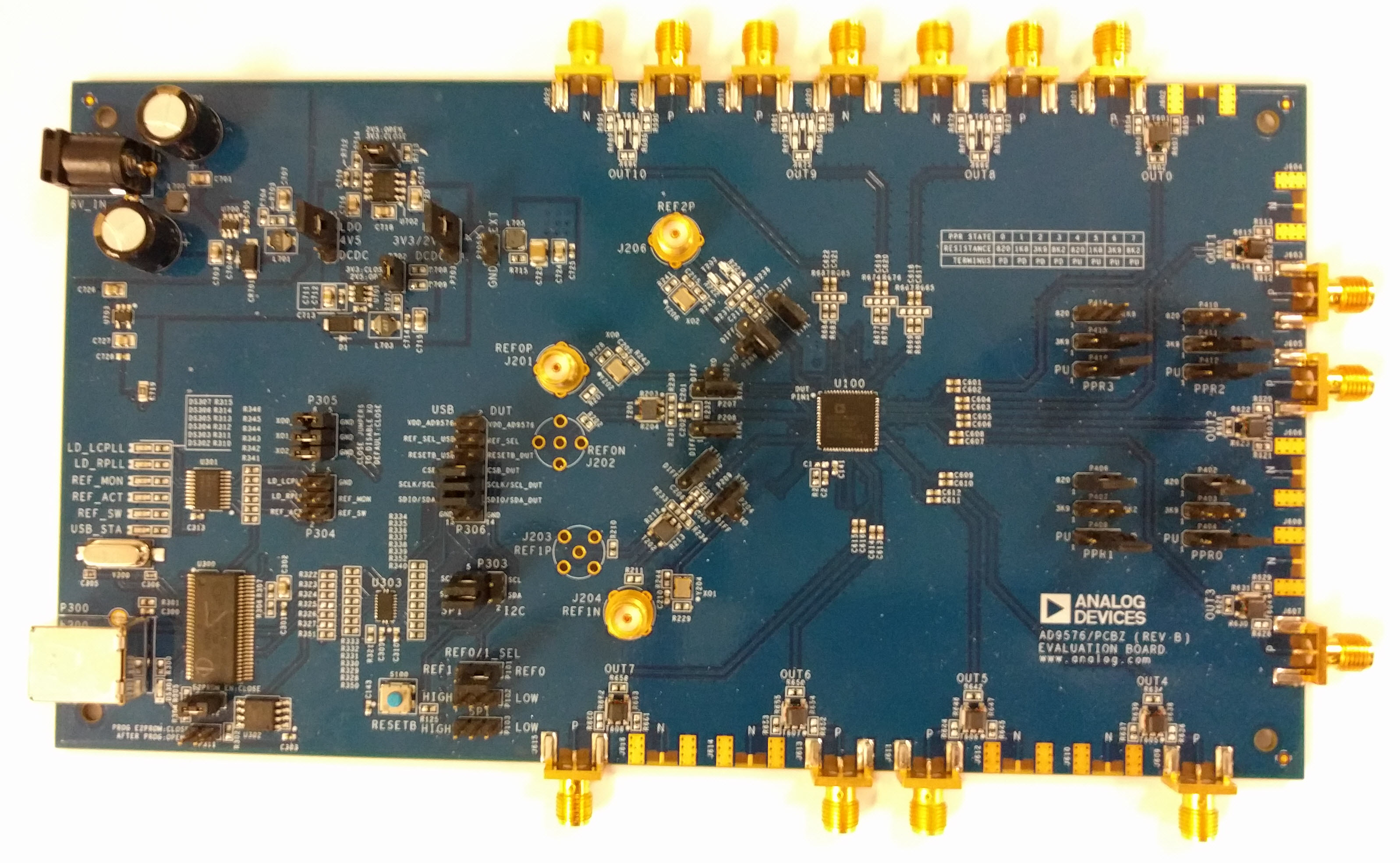
Figure 1. AD9576 Evaluation Board (AD9576/BCPZ)
EVALUATION BOARD HARDWARE
The following instructions are for setting up the physical connections to the AD9576/PCBZ evaluation board. The user must install the evaluation software prior to connecting the evaluation board for the first time.
Power Connections
The AD9576/PCBZ is setup by default to power the AD9576 and remaining circuitry using the provided 6V wall power supply connected to drive an Analog Devices ADM7151 Low Noise LDO configured to output 3.3V, but the evaluation board can be configured to power the AD9576 with one of five power configurations as shown in Table 1.
Table 1. Power Supply Configuration Jumper Settings
| Configuration Name | Settings | |||
|---|---|---|---|---|
| Jumper P701 | Jumper P702 | Jumper P703 | Jumper P704 | |
| 3.3V LDO powered by 4.5V ADP2300 Step-down Switching Regulator (Default) | Set to position 3 (LDO) | N/A | Set to position 3 (LDO) | Install Jumper |
| 2.5V LDO powered by 4.5V ADP2300 Step-down Switching Regulator | Set to position 3 (LDO) | N/A | Set to position 3 (LDO) | Remove Jumper |
| 3.3V ADP2300 Step-down Switching Regulator Direct | Set to position 1 (DCDC) | Install Jumper | Set to position 1 (DCDC) | N/A |
| 2.5V ADP2300 Step-down Switching Regulator Direct | Set to position 1 (DCDC) | Remove Jumper | Set to position 1 (DCDC) | N/A |
PC Connections
- Install all required software, uninstall prior versions of the software before installation updates. Administrative privileges are required for installation.
- Connect the 6V wall power supply to the main power connector labeled P700.
- Connect the USB cables to the evaluation board and the computer. The red LED labeled DS301 by the USB connector should illuminate and the LED labeled 'USB_STA' should blink.
- If the Found New Hardware Wizard window automatically appears when the evaluation board is connected, select Install the software automatically and click Next.
- The Found New Hardware Wizard window may appear twice, and a system restart may be required.
Refer to the Evaluation Board Software section for details on running the AD9576 evaluation board software.
Reference Inputs
The AD9576 evaluation has 3 reference inputs sources. The physical connection of each source is configurable between an on board XTAL, and on board XO, and an external reference input via SMA connector by configuring a set of 3 jumpers specific to the individual reference. Table 2 shows the jumper setting to configure the REF0 input connections.
Table 2. REF0 Configuration Jumper Settings
| REF0 Input Source | Settings | ||
|---|---|---|---|
| Jumper P202 | Jumper P207 | Jumper P208 | |
| XTAL | Removed | Position 3 (XTAL) | Position 3 (XTAL) |
| XO | Installed | Removed | Position 1 (DIFF) |
| External Input | Removed | Position 1 (DIFF) | Position 1 (DIFF) |
REF1 and REF2 may be configured in the same manner, but with jumper equivalencies shown in Table 3.
Table 3. Reference Input Configuration Jumper Equivalency
| REF 0 Jumper | Equivalent REF 1 Jumper | Equivalent REF2 Jumper |
|---|---|---|
| P202 | P204 | P206 |
| P207 | P209 | P211 |
| P208 | P210 | P212 |
Please note: Each AD9576 input receiver should be configured appropriately for signal applied. Please see the Reference Input section and Table 32 of the AD9576 data sheet for more information on this subject.
Serial Port Configuration Pins
The logic state of the AD9576 serial port configuration pins, SP0 and SP1, are read upon exit from a reset state and determine the protocol of the serial port as well as if a PPR load will be executed. P102 and P103 are connected to SP0 and SP1 respectively and Table 4 shows the effect of P102 and P103 states at release from a reset state.
Table 4. Serial Port configuration
| Jumper P103 | Jumper 102 | Serial Protocol | Slave Address | PPR Load? |
|---|---|---|---|---|
| Removed | Removed | SPI | N/A | Yes |
| Position 3 (LOW) | Removed | I 2C | 0x39 | Yes |
| Position 1 (HIGH) | Removed | I 2C | 0x3A | Yes |
| Removed | Position 3 (LOW) | I 2C | 0x3B | Yes |
| Position 3 (LOW) | Position 3 (LOW) | I 2C | 0x3C | Yes |
| Position 1 (HIGH) | Position 3 (LOW) | I 2C | 0x3D | Yes |
| Removed | Position 1 (HIGH) | I 2C | 0x3E | Yes |
| Position 3 (LOW) | Position 1 (HIGH) | I 2C | 0x3E | Yes |
| Position 1 (HIGH) | Position 1 (HIGH) | SPI | N/A | No |
PPRx Pins
The AD9576 uses pin strapping to select among a multitude of power-on ready configurations for its 11 output clocks, which require only the connection of external pull-up or pull-down resistors to the appropriate pin program reader pins (PPRx). These pins configure the internal registers for establishing the desired frequency translations, clock output functionality, and input reference functionality.
Each PPR pin can be individually configured between all applicable impedance and terminus values by configuring a set of 3 jumpers specific to the individual reference. Table 5 shows the jumper setting to configure the REF0 input connections.
Table 5. PPR0 State Jumper Settings
| PPR0 State | Settings | ||
|---|---|---|---|
| Jumper P402 | Jumper P403 | Jumper P404 | |
| 0 | Position 1 (820) | Removed | Position 3 (PD) |
| 1 | Position 3 (1K8) | Removed | Position 3 (PD) |
| 2 | Removed | Position 1 (3K9) | Position 3 (PD) |
| 3 | Removed | Position 3 (8K2) | Position 3 (PD) |
| 4 | Position 1 (820) | Removed | Position 1 (PU) |
| 5 | Position 3 (1K8) | Removed | Position 1 (PU) |
| 6 | Removed | Position 1 (3K9) | Position 1 (PU) |
| 7 | Removed | Position 3 (8K2) | Position 1 (PU) |
PPR1, PPR2, and PPR3 may be configured in the same manner, but with jumper equivalencies shown in Table 6.
Table 6. PPRx State Jumper Equivalency
| PPR0 Jumper | Equivalent PPR1 Jumper | Equivalent PPR2 Jumper | Equivalent PPR3 Jumper |
|---|---|---|---|
| P402 | P406 | P410 | P414 |
| P403 | P407 | P411 | P415 |
| P404 | P408 | P412 | P416 |
Used in conjunction with the PPR tables (Table 31 - Table 34) in the AD9576 data sheet, these pins allow the user to set the AD9576 to a multitude of power on ready configurations provided the serial port configuration pins are configured to allow a PPR load.
Please note: The AD9576 input receivers physical connections should be configured to match the reference input format configured by PPR0 and the AD9576 outputs should be terminated to match the output logic formats determined by PPR1, PPR2, and PPR3.
RESETB Push Button
The blue RESETB push button, S100, is located in the lower left quadrant of the board. When this button is depressed, the AD9576 is held in a chip level reset state. This push button may be used to reconfigure the logic levels read by the AD9576 for the serial port configuration pins and PPRx pins. Please note: This push button is a board level operation and the evaluation software is unaware of its operation. Therefore, using this push button will desynchronize the state of the AD9576 with the state of the evaluation board software. To re-establish synchronization, one must press the READ ALL button in the AD9576 Chip View window.
EVALUATION BOARD SOFTWARE
The AD9576 evaluation software allows the user to control the full functionality of the AD9576 through SPI communication with the evaluation board. The AD9576 evaluation software is implemented as a component plug-in in ADI’s Analysis | Control | Evaluation (ACE) Software desktop software. ACE allows the evaluation of control of multiple evaluation systems from across ADI’s product portfolio and is designed to educate the user in the functional operation of the component. The ACE wiki page contains system requirement and prerequisite information as well as links to the most recent installer and user guide. The ACE user guide contains detailed information concerning all current aspects of the ACE environment. Much of that information will not be described in this document, but some main ACE operational points relevant to component level functionality will be described. It is highly recommended to review the ACE user guide to discover the myriad capabilities and offerings the ACE environment provides to the user.
Software Installation
Use the following instructions to set up the AD9576 evaluation board software. Do not connect the evaluation board until the software installation is complete.
- Download the AD9576 driver installer, ADI_LRF_CYUSBdriver.exe, from the AD9576 Evaluation product page.
- Run the installer and follow the prompts through completion.
- Download the ACE software installer.
- Follow the section 2.1, installation guide, of the ACE User Guide to completion.
General Operation
Power up and connect the evaluation board to the PC. Open the ACE software. After opening ACE, the user will be presented with the Start View shown in Figure 2. The Explore Local Plug-ins section shows all plug-ins that are locally installed and allows the user to operate the plug-in without the presence of the associated evaluation platform. The Attached Hardware section shows all ADI evaluation platforms which are found to be connected to the PC. The appearance of an Unknown Hardware plug-in means that the plug-in for a detected ADI evaluation platform is not locally installed. Double click on any of the shown plug-ins will open the associated plug-in and navigate to its default view, which is the board view for the AD9576. Note: opening a plug-in from the Explore Local Plug-ins section will not automatically establish a connection with the associated evaluation platform even if the hardware is connected. Only opening a plug-in from the Attached hardware section will automatically establish this connection.

Figure 2. ACE Start Screen
Board View
The AD9576 board view can be seen in Figure 3. As the AD9576 evaluation platform is for a single component, the board view has only three main portions, each circled and numbered in Figure 3:
- View toolbar
- AD9576 primaray component link
- PPR pin state jumper truth table

Figure 3. AD9576 ACE Plug-in Board View
The board view toolbar provided three board level functions and a detailed description may be found in section 3.6.3 of the ACE user guide. The AD9576 primary component link allows the user to navigate to the AD9576 chip view, shown in Figure 4, by double clicking this link. The chip view is the primary conduit through which the user can interface with the AD9576. The PPR pin state jumper truth table shows the user the jumper configuration to place a given PPR pin into a PPR state. Used in conjunction with the PPR tables (Table 31 - Table 34) in the AD9576 data sheet, the user can set the AD9576 to a multitude of power on ready configurations. Please note that the SP0 and SP1 jumpers must be configured to allow a PPR load.
Chip View
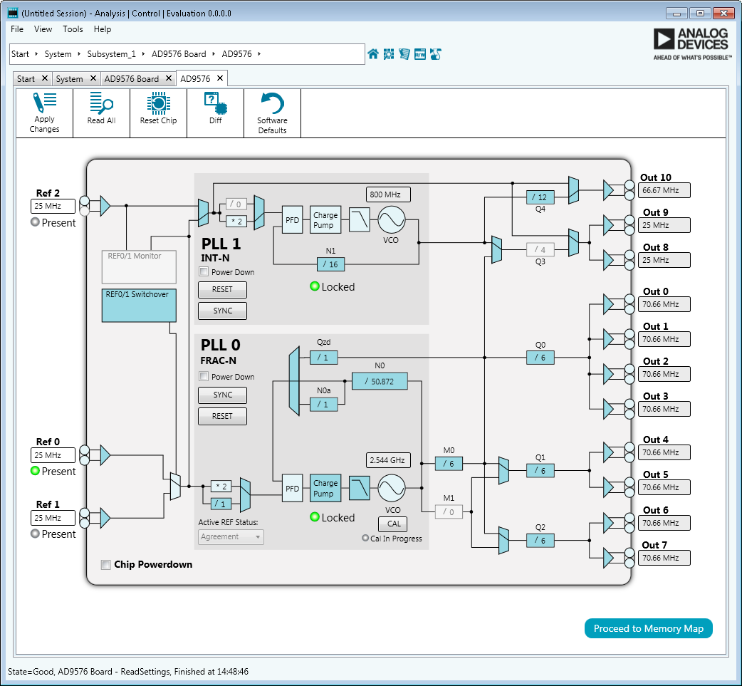
Figure 4. AD9576 ACE Plug-in Chip View
The chip view is the primary interface used to configure the AD9576. It consists primarily of an interactive block diagram which shows the configuration of the device, calculates the frequency translation, implements frequency based error checking, and allows the user to intuitively configure the AD9576 parameters. It should be noted that in order to synchronize the register content of the software with that of the AD9576 after a PPR load, the user must press the ‘Read All’ button in the chip view toolbar in the upper left hand portion of the window.
Block Interaction
A detailed explanation of the interaction with the block diagram is explained in the ACE User Guide sections 3.7.1 through 3.7.3. However, it should be noted that the AD9576 chip view heavily leverages the use of configuration menus for blocks with multiple associated bit fields. Clicking on such a block will pop up a menu as pictured in Figure 5.
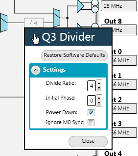
Figure 5. Divider Q3 configuration menu
Clicking and dragging the title bar of the menu will allow the user to relocate the menu at one’s convenience. In order to close the menu, the user may close the ‘close’ button or simply click away from the menu.
Frequency Translation Calculations
The frequency translation of the AD9576 is calculated from reference input frequency to output clock frequency based on the state of the intermediate blocks in between. Not every block in the block diagram impacts the frequency translation, but those that do contain a tool tip displaying the input and output frequencies associated with said block as illustrated in Figure 6.

Figure 6. Frequency display tool tip.
Changing the configuration of a block that affects the frequency translation will produce an automatic calculation and error checking to inform the user of the impact the change has had on the operation of the AD9576. Any errors resulting from the error checking functionality will display visually as well as the Events Tool View. This view gives the user additional detail regarding the nature of the error and is explained in detail in the ACE User Guide, section 3.9.3.
Memory Map View
The AD9576 ACE plug-in as contains a detailed view of the entire register map in either register or bit field based format, known as the Memory Map shown in Figure 7. This view may be accessed by clicking the ‘Proceed to Memory Map’ button in the lower right hand corner of the chip view.

Figure 7. AD9576 ACE Plug-in Memory Map View.
The memory map view is explained in detail in the ACE User Guide section 3.8, but one of the more useful features in the functional group filter shown in the left portion of Figure 7. The AD9576 bit fields have been grouped by relevant functionality and the functional group filter allows the user to quickly and easily switch between viewing only bit fields or registers contained within these macro level functional groups.
Sessions
The ACE application has the ability to save and recall a given configuration of the software including all currently open plug-ins. These ‘states’ are referred to as ‘sessions’. The File selection in the application toolbar contains options to create, open, save, or close sessions, as shown in Figure 8.

Figure 8. ACE File Menu.
The left hand section of the Start View also exposes the ability to create and open sessions as well as maintaining a list of recent sessions that may be directly opened.
Known Issues
- Though the AD9576 supports I 2C communication, currently the ACE application does not support the usage of the I 2C portion of the AD9576 drivers.
- Currently, the ACE AD9576 plug-in does not support the control or read back of the AD9576 evaluation board GPIO pins.
EVALUATION BOARD QUICK START
Power-on Ready Configuration
This quick start section covers only configuring the AD9576 to execute a PPR load to configure the AD9576 according to Typical Configuration 1 (Asynchronous operation) as outlined in Table 3 of the AD9576 data sheet.
- Remove any jumpers on P102 and P103 to configure the AD9576 for SPI communication with a PPR load.
- Short pin 1 and pin 2 on P402, remove any jumpers from P403, and short pin 2 and pin 3 on P404 to set PPR0 to state 0.
- Short pin 1 and pin 2 on P406, remove any jumpers from P407, and short pin 2 and pin 3 on P408 to set PPR1 to state 0.
- Remove any jumpers from P410, short pin 2 and pin 3 on P411, and short pin 2 and pin 3 on P412 to set PPR2 to state 3.
- Remove any jumpers from P414, short pin 2 and pin 3 on P415, and short pin 2 and pin 3 on P416 to set PPR3 to state 3.
- Short pin 2 and pin 3 on P207, P208, P209, and P210 to configure both REF0 and REF1 for 25 MHz XTAL inputs.
- Issue a chip level reset by pressing the RESETB push button, S100, or power cycling the evaluation board. This may optionally be done from the ACE software as well.
- VCO0 will automatically calibrate and all outputs will toggle.
- To view the register configuration, open the ACE software and navigate to the AD9576 Chip View.
- Press the ‘Read All’ button in the Chip View Toolbar to synchronize the software to the connected device. The Chip View will appears as that featured in Figure 9.

Figure 9. AD9576 Asynchronous Operation Configuration
Session Based Configuration
This quick start section covers only the AD9576 Typical Configuration 2 (Synchronous operation) as outlined in Table 3 of the AD9576 data sheet.
- Ensure the Serial Port Configurations Pins, SP0 and SP1, are configured for SPI communication on board power up.
- Short pin 1 and pin 2 of P207 and P208 to configure REF0 for a differential input and short pin 2 and pin3 of P211 and P212 to configure REF2 for a XTAL input.
- Download the AD9576 Quick Start Session file ‘ad9576_typical_configuration_2.cso’ from the AD9576 evaluation page.
- Once downloaded, the session file can be loaded into the evaluation board by opening the ACE Evaluation Software, click File > Open Session…, and select the appropriate .cso file.
- In the AD9576 Chip View Toolbar, click the Apply Changes button.
- Apply a 100 MHz, 0 dBm signal to the J201 SMA connector (REF0P). This may also be applied prior to the session load.
- The VCO0 calibration will trigger automatically once the reference is detected and the PLL0 locked indicator will turn green and all enabled outputs will toggle.

Figure 10. AD9576 Synchronous Operation Configuration
resources/eval/ad9576-user-guide.1472232078.txt.gz · Last modified: 26 Aug 2016 19:21 by Neil Weeks