


This version is outdated by a newer approved version. This version (09 Mar 2015 18:44) was approved by Kyle Slightom.The Previously approved version (09 Apr 2013 14:49) is available.
This version (09 Mar 2015 18:44) was approved by Kyle Slightom.The Previously approved version (09 Apr 2013 14:49) is available.This is an old revision of the document!
Table of Contents
AD9508 Evaluation Board User Guide
Evaluation Board Features
- Simple power connection using 6 V wall adapter and on-board LDO voltage regulators
- 8 ac-coupled single-ended SMA output connectors
(4 differential paths) - 2 ac-coupled single-ended SMA connectors for reference input
- Pin selectable options for the following:
- 2.5 V or 3.3 V operation
- SPI/I2C or Sx pin programmable
- OUT0 through OUT3 divide value
- OUT0 through OUT3 logic type
- Input logic type
- USB connection to PC
- Microsoft Windows-based evaluation software with simple graphical user interface (supports 64-bit versions of Windows)
Equipment Needed
- Reference oscillator or signal generator
- Other evaluation board to be clocked or test equipment
- Converters, DDS, transceivers
- Oscilloscope, spectrum analyzer, phase noise analyzer
- SMA cables (50 Ω)
- 6 V wall supply (provided)
- USB cable (provided)
Online Resources
General Description
The AD9508 evaluation board is a compact, easy-to-use platform for evaluating all features of the AD9508. This user guide focuses on the AD9508 evaluation board and software. The AD9508 is a high performance 1:4 flexible clock buffer. Each output has a programmable divider that can be set via SPI/I2C programming or Sx pin strapping. The AD9508 features both 2.5 V and 3.3 V operation. For convenience, detailed information from the AD9508 data sheet has been included in this user guide. Use this guide in conjunction with the AD9508 data sheet and software documentation available at www.analog.com.

Figure 1. AD9508/PCBZ
Evaluation Board Hardware
The following instructions are for setting up the physical connections to the AD9508/PCBZ evaluation board. Before connecting the evaluation board to a PC for the first time, the user must install the evaluation software.
Power and PC Connections
- Before installing the AD9508 evaluation software, uninstall prior versions of the software. Administrative privileges are required for installation. The 64-bit versions of Windows® are supported.
- Connect the 6 V wall power supply to the main power connector labeled P500.
- Connect the USB cable to the evaluation board and the computer. The red LED labeled CR300 on the AD9508 evaluation board should illuminate.
- If the Found New Hardware Wizard window appears when the evaluation board is connected, select Install the software automatically and click Next. The Found New Hardware Wizard window may appear twice, and a system restart may be required.
- After the driver software has installed, the red LED labeled CR301 blinks.
Signal Connections
To connect signals, connect a signal generator to the J200 (CLKIN) SMA connector. By default, the CLKIN input is connected to a balun for single-ended to differential conversion. This path is differentially terminated to 100 Ω and ac-coupled into the AD9508 reference inputs. An amplitude setting of 0 dBm to 6 dBm is fine. The CLKIN_B SMA input is grounded by default. To input a differential signal, the user must remove Balun T200 and Resistor R221, and replace Resistors R209 and R210 with 0 Ω. Connect an oscilloscope, spectrum analyzer, or other lab equipment to any of the J209 to J216 SMA clock OUTx connectors on the edge of the board. OUT0 through OUT3 are ac-coupled outputs differentially terminated to 100 Ω.
Pin Programming and Jumper Settings
Jumpers P507, P100, and P101
- Jumper P507 allows the user to select between 2.5 V and 3.3 V operation.
- Jumper P100 allows the user to select between differential and single-ended inputs.
- Jumper P101 allows the user to select the programming method (SPI/I2C/Sx pin programming) to be used by the AD9508. Placing no jumper defaults the part to use the SPI. I2C programming is not currently supported with the evaluation board software. When pin programming is selected, Pin S0 through Pin S5 are used to determine various divider ratios and output modes for each of the AD9508 outputs. Using the Sx pins to program the part gives the user limited control of each channel divider ratio and no control of phase offset. Refer to the AD9508 data sheet for a complete overview regarding the use of the part with Sx pin programming.
Jumpers P102, P106, P110, and P114
- Jumpers P102, P106, P110, and P114 connect and disconnect Pin S0 through Pin S3 to a SPI/I2C line. These must be set with respect to the setting of P101. Table 1 describes the proper placement of these jumpers.
Table 1. P102, P106, P110, and P114 Jumper Settings with Respect to Jumper P101 Setting
| Programming Pin | Jumper Placement vs. Programming Method (SPI or I2C) | Pin Strapping |
|---|---|---|
| S0 | P102 = SCLK | P102 = S0P |
| S1 | P106 = SDIO | P106 = S1P |
| S2 | P110 = | P110 = S2P |
| S3 | P114 = SDO | P114 = S3P |
There are two more jumpers allocated for each Sx pin that are used to obtain all eight divider settings (for Pin S0 through Pin S3) and to select between logic types (Pin S4 and Pin S5). The first jumper is used to pull the Sx pin up to VDD or down to GND. The second jumper is used to select one of the four resistor settings on the evaluation board. Table 2 describes the possible divider and output mode settings when in Sx pin programming mode. Table 3 lists the jumper label associated with each divider ratio and driver mode setting.
Table 2. Divider Ratio and Driver Mode Table for S0, S1, S2, S3, S4, and S5 Pins (Driver Modes Are Listed in the Order of CH1/CH2 or CH3/CH4)
| Programming Pins | Sx Pin Settings (0 Through 7) vs. Resistor Value vs. Divide Value and Logic Type | Description | |||||||
|---|---|---|---|---|---|---|---|---|---|
| 0 = 820 Ω Pulled to GND | 1 = 1.8 kΩ Pulled to GND | 2 = 3.9 kΩ Pulled to GND | 3 = 8.2 kΩ Pulled to GND | 4 = 820 Ω Pulled to VDD | 5 = 1.8 kΩ Pulled to VDD | 6 = 3.9 kΩ Pulled to VDD | 7 = 8.2 kΩ Pulled to VDD | ||
| S0 | ÷1 | ÷2 | ÷3 | ÷4 | ÷5 | ÷6 | ÷8 | ÷16 | S0 is assigned to the CH0 divider ratio only |
| S1 | ÷1 | ÷2 | ÷3 | ÷4 | ÷5 | ÷6 | ÷8 | ÷16 | S1 is assigned to the CH1 divider ratio only |
| S2 | ÷1 | ÷2 | ÷3 | ÷4 | ÷5 | ÷6 | ÷8 | ÷16 | S2 is assigned to the CH2 divider ratio only |
| S3 | ÷1 | ÷2 | ÷3 | ÷4 | ÷5 | ÷6 | ÷8 | ÷16 | S3 is assigned to the CH3 divider ratio only |
| S4 | HSTL/HSTL | HSTL/LVDS | HSTL/ Disable | LVDS/HSTL | LVDS/ LVDS | LVDS/ Disable | Disable/ HSTL | Disable/ Disable | S4 is assigned to CH0/CH1 to select their output logic types |
| S5 | HSTL/HSTL | HSTL/LVDS | HSTL/ Disable | LVDS/HSTL | LVDS/ LVDS | LVDS/ Disable | Disable/ HSTL | Disable/ Disable | S5 is assigned to CH2/CH3 to select their output logic types |
Table 3. Evaluation Board Sx Pin Jumper Labels
| Programming Pins | Evaluation Board Sx Pin Jumper Labels | ||
|---|---|---|---|
| 820 Ω/1.8 kΩ | 3.9 kΩ/8.2 kΩ | Pull Up to VDD/Pull Down to GND | |
| S0 | P103 | P104 | P105 |
| S1 | P107 | P108 | P109 |
| S2 | P111 | P112 | P113 |
| S3 | P115 | P116 | P117 |
| S4 | P118 | P119 | P120 |
| S5 | P121 | P122 | P123 |
Evaluation Board Software
The AD9508 evaluation software allows the user to control the full functionality of the AD9508 through SPI/I2C communication on the evaluation board. Use the following instructions to set up the evaluation board software.
Software Installation
Do not connect the evaluation board until the software installation is complete.
- The latest evaluation software and documentation can be downloaded from http://www.analog.com/eval-ad9508.
- On the AD9508 evaluation board page, under Software and Tools, click Evaluation Board AD9508 - Web Install or Evaluation Board AD9508 - Full Install. The full version of the installer is a much larger file that contains the entire standalone installation for the .NET framework, and it does not require an Internet connection. The web installer contains an executable that can download the .NET framework, but this does require an Internet connection. However, if the .NET framework has already been installed, an Internet connection is not required to proceed.
- Follow the installation instructions.
Running the Software
Power up and connect the evaluation board to the PC. See the Evaluation Board Hardware section for details on the various connectors on the evaluation board.
- Windows may automatically detect the evaluation board after the board is first plugged in. Allow Windows to install the device drivers.

Figure 2. Device Hardware Installation - Double-click AD9508 Evaluation Software to run the AD9508 software. If the evaluation board is found by the software, the lower left corner of the main window (see Figure 4) displays AD9508 Evaluation Board in green. If the evaluation board is not found, the lower left corner of the window displays No Hardware Connected! in red.
- If the evaluation board is found, proceed to the Evaluation Software Components section for details about running the software. If the evaluation board is not found, click File > Select Hardware. Select the appropriate AD9508 evaluation board connected and click OK (see Figure 3).

Figure 3. Select Hardware Window

The bottom left corner of the main window should now display AD9508 Evaluation Board in green. Alternatively, you can use the software in standalone mode. The standalone mode is useful for verifying register settings for a given setup. See the Evaluation Software Components section for a description of the evaluation software features.
Evaluation Software Components
Main Window
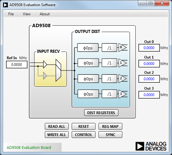
Figure 4. Evaluation Software Main Window
The AD9508 evaluation software is composed of subsections that correspond to the major functional blocks of the AD9508. These subsections are described in the following sections of the user guide. Some of the subsections have dedicated windows that allows the user to edit the register settings associated with a functional block. For example, the output distribution functional block window can be accessed by clicking the DIST REGISTER button. Some of the functional blocks have editable text areas that can be accessed and altered without opening each functional block window. Altering these text areas changes the settings found in the various block windows and immediately loads the change into the evaluation board. Conversely, edits to the settings within a block are reflected in the respective text area.
After clicking Load, the settings from that subwindow are loaded to the evaluation board. When editing a text box within the main window, the ENTER key must be pressed before a change is saved and loaded into the evaluation board.
Input Receiver
The input receiver (INPUT RECV) section allows the user to select between single-ended and differential operation. Click the mux symbol within the block to highlight the active path (see Figure 5). The left image in Figure 5 shows the default differential operation of the input receiver. The right image shows single-ended operation.


Figure 5. Input Receiver Section
Left Image: Default Differential Operation of Input Receiver; Right Image: Single-Ended Operation
Output Distribution
The output distribution (OUTPUT DIST) section allows the user to alter divide ratios and phase offsets for each output of the AD9508. Each divide and phase block can be edited by typing the preferred value within the block, and then pressing the ENTER key. When ENTER is pressed, the values are loaded into the evaluation board. The phase offset blocks accept the u (micro), p (pico), and n (nano) prefixes. Phase offset is limited to one half of the period of the input clock rate. Each divider supports integer divide values from 1 to 1024. If the typed value is not achievable in the current configuration, the software automatically rounds to the nearest possible solution. The output distribution section is shown in Figure 6.
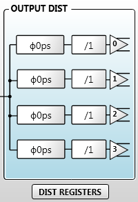
Figure 6. Output Distribution Section
Clicking the DIST REGISTERS button at the bottom of the output distribution section allows the user to access all of the distribution register settings in the Distribution Settings window (see Figure 7).

Figure 7. Distribution Settings Window
The Distribution Settings window consists of four individual tabs for each output channel. Each tab contains controls for each channel divide ratio, phase offset, driver mode, polarity and power-down settings. To load any of the settings to the evaluation board changed within the Distribution Settings window, the user must click the Load button.
The driver mode and polarity settings are altered by selecting one of the values from the respective drop-down box and clicking the Load button. To power down a channel driver, the appropriate channel power-down box must be selected.
Operational Controls Window
The Operational Controls window is opened by clicking the CONTROL button at the bottom of the main window. This window contains controls for SPI configuration, LDO voltage control, channel power-down, sleep mode, and two buttons for soft reset and soft sync. The Operational Controls window is shown in Figure 8.
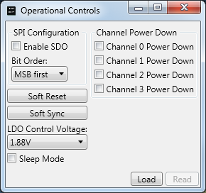
Figure 8. Operational Controls Window
Register Map Window
The Register Map window is accessed by clicking the REG MAP button at the bottom of the main window. Figure 9 shows the Register Map window.

Figure 9. Register Map Window
The Register Map window contains two tabs. The All tab displays all of the registers that can be changed through the AD9508 evaluation software. Each register can be selected by clicking the various blue boxes shown in Figure 9. Register details for the selected register appear at the bottom of the window. These details include the name of the register, the current register value, and the various bit fields for the register. The Changed tab contains all of the registers that have been modified from within the AD9508 evaluation software but not loaded into the evaluation board yet. These same registers are also highlighted in the All tab as they are modified.
READ ALL and WRITE ALL Buttons
The READ ALL and WRITE ALL buttons are located at the bottom of the main window. Click the READ ALL button to read all of the register values currently stored in the chip and transfer them to the evaluation software. Click the WRITE ALL button to transfer all of the register values currently loaded into the software and write them to the chip.
Reset Button
The Reset Button is located at the bottom of the main window. Clicking this button resets the part to its default register settings, which is also reflected in the main window.
SYNC Button
Click the SYNC button to issue a soft synchronization command, which synchronizes all outputs that are not omitted by the appropriate SYNCMASKx bit. Refer to the AD9508 data sheet for more information about the sync command.
Evaluation Software Menu Items

Figure 10. Menu Bar
File Menu
The File menu includes the following options:
- Load Setup
- Save Setup
- Select Hardware
- Options
- Enable Polling
- Polling Interval
- Exit
Load Setup
Selecting Load Setup loads a previously saved AD9508 setup file (.stp). A setup file is a text file that contains the AD9508 register setup file, plus any evaluation board settings.
Save Setup
Selecting Save Setup saves an AD9508 setup file (.stp). A setup file is a text file that contains the AD9508 register settings, plus any evaluation board settings.
Select Hardware
The AD9508 evaluation system allows one PC to control multiple evaluation boards. This window allows the user to select the evaluation board that the software is controlling. Click the Refresh button to detect a recently connected evaluation board.
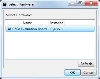
Figure 11. Select USB Device Window
Options (Enable Polling and Polling Interval)
Polling allows the user to define how often the software checks for changes made to the register values on the AD9508. Polling also checks for a hardware connection, which updates in the lower left corner of the main window. The polling interval window sets the length of time between each software check. The default interval is 1 sec. Figure 12 shows the polling interval selection window.
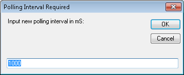
Figure 12. Polling Interval Window
Exit
Exits the evaluation software. No checking is performed to ensure that the existing setup is saved.
View Menu
The View menu includes the following options:
- Register Map
- Debug
Register Map
Opens the Register Map window. See the Register Map Window subsection in the Evaluation Software Components section.
Debug
The Debug window allows the user to read the values that are loaded into the various register addresses as well as manually load values into each register address of the AD9508 on the evaluation board. Figure 13 shows the Debug Window. Detailed information about the usable registers and their functions can be found in the AD9508 data sheet.

Figure 13. Debug Window
About Menu
Selecting About opens the AD9508 window, which contains information about the version of the evaluation board software.
I2C refers to a communications protocol originally developed by Philips Semiconductors (now NXP Semiconductors).
resources/eval/ad9508-user-guide.1425922755.txt.gz · Last modified: 09 Mar 2015 18:39 by Kyle Slightom