


This version (03 Dec 2021 03:08) was approved by Meriam Yuson-Aguila.The Previously approved version (26 Oct 2021 11:21) is available.
Table of Contents
EVALUATING THE AD9484 / AD9601 / AD9230 / AD9211 / AD9626 ANALOG-TO-DIGITAL CONVERTER
Preface
This user guide describes the AD9484, AD9601, AD9230, AD9211 and AD9626 evaluation boards, AD9484-500EBZ, AD9601-250EBZ, AD9230-250EBZ, AD9211-300EBZ and AD9626-250EBZ which provide all of the support circuitry required to operate these parts in their various modes and configurations. The application software used to interface with the devices is also described.
The AD9484, AD9601, AD9230, AD9211 and AD9626 data sheets provide additional information and should be consulted when using the evaluation board. All documents and software tools are available at www.analog.com/hsadcevalboard. For additional information or questions, send an email to highspeed.converters@analog.com.
Typical Measurement Setup

Figure 1. Evaluation Board Connection—AD9484-500EBZ, AD9601-250EBZ, AD9230-250EBZ, AD9211-300EBZ or AD9626-250EBZ (on Left) and HSC-ADC-EVALCZ (on Right)
Features
- SPI interface for setup and control
- External, on-board oscillator, or AD9517 clocking option
- Balun/transformer or amplifier input drive option
- LDO regulator or switching power supply options
- VisualAnalog® and SPI controller software interfaces
Helpful Documents
- High speed ADC FIFO evaluation kit (HSC-ADC-EVALCZ)
- AN-905 Application Note, VisualAnalog Converter Evaluation Tool Version 1.0 User Manual
- AN-878 Application Note, High Speed ADC SPI Control Software
- AN-877 Application Note, Interfacing to High Speed ADCs via SPI
- AN-835 Application Note, Understanding ADC Testing and Evaluation
Design and Integration Files
- Schematics: AD9230-250EBZ RevC
- Bill of Materials: AD9230-250EBZ RevC
- PCB Gerber files: AD9230-250EBZ RevC
Equipment Needed
- Analog signal source and antialiasing filter
- Sample clock source (if not using the on-board oscillator)
- 2 switching power supplies (6.0 V, 2.5 A), CUI EPS060250UH-PHP-SZ provided
- PC running Windows®
- USB 2.0 port
- HSC-ADC-EVALCZ FPGA-based data capture kit
Getting Started
This section provides quick start procedures for using the AD9484-500EBZ, AD9601-250EBZ, AD9230-250EBZ, AD9211-300EBZ or AD9626-250EBZ board. Both the default and optional settings are described.
Configuring the Board
Before using the software for testing, configure the evaluation board as follows:
- Connect the evaluation board to the data capture board, as shown in Figure 1.
- Connect one 5 V, 3 A (6 V, 2 A can optionally be used) switching power supply (such as the supplied CUI KSAFD0500300W1US supplied) to the HSC-ADC-EVALCZ board.
- Connect the HSC-ADC-EVALCZ board to the PC with a USB cable. (Connect to J6)
- On the ADC evaluation board, confirm that the jumpers are on the J300 to J303 headers to connect the power supplies. Connect Pin 1 to Pin 2 of P200 and Pin 2 to Pin 3 of P400 to connect SPU bus to the ADC.
- On the ADC evaluation board, provide a clean, low jitter clock source to connector J200 at the desired ADC conversion rate.
- On the ADC evaluation board, use a clean signal generator with low phase noise to provide an input signal at the J100 connector. Use a 1 meter, shielded, RG-58, 50 Ω terminations and an appropriate center frequency. (Analog Devices uses TTE, Allen Avionics, and K & L band-pass filters.)
Evaluation Board Hardware
The evaluation board provides the support circuitry required to operate the AD9484, AD9601, AD9230, AD9211 and AD9626 in their various modes and configurations. Figure 1 shows the typical bench characterization setup used to evaluate AC performance. It is critical that the signal sources used for the analog input and clock have very low phase noise (<1 ps rms jitter) to realize the optimum performance of the signal chain. Proper filtering of the analog input signal to remove harmonics and lower the integrated or broadband noise at the input is necessary to achieve the specified noise performance.
See the Getting Started section to get started, and Design and Integration Files sections for the complete schematics and layout diagrams. These diagrams demonstrate the routing and grounding techniques that should be applied at the system level when designing application boards using these converters.
Power Supplies
This evaluation board comes with a wall-mountable switching power supply that provides a 6 V, 2 A maximum output. Connect the supply to a 100 V ac to 240 V ac, 47 Hz to 63 Hz wall outlet. The output from the supply is provided through a 2.1 mm inner diameter jack that connects to the printed circuit board (PCB) at J300. The 6 V supply is fused and conditioned on the PCB before connecting to the low dropout linear regulators (default configuration) that supply the proper bias to each of the various sections on the board.
The evaluation board can be powered in a nondefault condition using external bench power supplies. To do this, JP301 through JP303 can be removed to disconnect the outputs from the on-board LDOs. This enables the user to bias each section of the board individually. Use P300 and P301 to connect a different supply for each section. A 1.8 V supply is needed with 1A current capability for DUT_AVDD and DRVDD; however, it is recommended that separate supplies be used for both analog and digital domains. To operate the evaluation board using the SPI and alternate clock options, a separate 3.3 V analog supply is needed in addition to the other supplies. This 3.3 V supply should have a 1 A current capability.
An additional 5V_AVDD is used to bias the optional input path amplifier. If used, this supply should each have 1 A current capability.
Input Signals
When connecting the ADC clock and analog source, use clean signal generators with low phase noise, such as the Rohde & Schwarz SMA, or HP 8644B signal generators or an equivalent. Use a 1 m shielded, RG-58, 50 Ω coaxial cable for connecting to the evaluation board. Enter the desired frequency and amplitude in the signal generators (see the Specifications section in the data sheet of the respective part). When connecting the analog input source, use of a multipole, narrow-band band-pass filter with 50 Ω terminations is recommended. Analog Devices uses band-pass filters from TTE, Allen Avionics and K & L Microwave, Inc. Connect the filters directly to the evaluation board.
If an external clock source is used, it should also be supplied with a clean signal generator as previously specified. Analog Devices evaluation boards typically can accept ~2.8 V p-p or 13 dBm sine wave input for the clock.
Output Signals
The default setup uses the Analog Devices high speed converter evaluation platform (HSC-ADC-EVALCZ) for data capture. The serial LVDS outputs from the ADC are routed to the FPGA on the data capture board. For more information on the data capture board and its optional settings, visit www.analog.com/hsadcevalboard.
Default Operation and Jumper Selection Settings
This section explains the default and optional settings or modes allowed on the AD9484, AD9601, AD9230, AD9211 and AD9626 evaluation boards.
Power Circuitry
Connect the switching power supply that is supplied in the evaluation kit between a rated 100V to 240V ac wall outlet (at 47 Hz to 63 Hz) and J300.
Analog Input
The input on the evaluation board is set up for a double balun-coupled analog input with a 50 Ω impedance. The analog input to the AD9484, AD9601, AD9230, AD9211 and AD9626 is a differential buffer. For best dynamic performance, source impedances driving VIN+ and VIN- are matched such that common-mode settling errors are symmetrical. The analog input is optimized to provide superior wideband performance and requires that the analog inputs be driven differentially. SNR and SINAD performance degrades significantly if the analog input is driven with a single-ended signal.
The analog inputs are self-biased by an on-chip reference to provide a common-mode voltage level of nominally 1.7V.
An internal differential voltage reference creates positive and negative reference voltages that define the 1.5 V p-p fixed span of the ADC core. This internal voltage reference can be adjusted by means of an SPI control.
VREF
The AD9484 VREF pin (Pin31) allows the user to monitor the on-board voltage reference or provide an external reference (requires configuration through SPI). The three optional settings are internal Vref (the pin is connected to 20 kΩ to ground), export Vref, and import Vref. See Memory Map section in the data sheet.
RBIAS
The AD9601, AD9230, AD9211 and AD9626 RBIAS pin (Pin31) has a default setting of 10 kΩ (R205) to ground and is used to set the ADC core bias current. Note that using a resistor value other than a 10 kΩ, 1% resistor for RBIAS may degrade the performance of the device.
Clock Circuitry
The default clock input circuit on the evaluation board uses a simple transformer-coupled circuit using a high bandwidth 1:1 impedance ratio transformer (T201) that adds a low amount of jitter to the clock path. The clock input is 50 Ω terminated and ac-coupled to handle single-ended sine wave types of inputs. The transformer converts the single-ended input to a differential signal that is clipped by CR200 before entering the ADC clock inputs.
The evaluation board is by default set up to be clocked with the transformer-coupled input network connected to the external clock source through the SMA connector, J200 (labeled CLK+).
PDWN
To enable the power-down feature, add a shorting jumper across P200 at Pin 1 and Pin 2 to connect the PDWN pin to AVDD.
Using The Software for Testing
Setting up the ADC Data Capture
After configuring the board, set up the ADC data capture using the following steps:
- Open VisualAnalog on the connected PC. The appropriate part type should be listed in the status bar of the VisualAnalog – New Canvas window. Select the template that corresponds to the type of testing to be performed (see Figure 2, where the AD9230 is shown as example).

Figure 2. VisualAnalog, New Canvas Window
- To change features to settings other than the default settings, click the Expand Display button, located on the bottom right corner of the window (see Figure 3), to see what is shown in Figure 4.
- Detailed instructions for changing the features and capture settings can be found in the AN-905 Application Note, VisualAnalog Converter Evaluation Tool Version 1.0 User Manual. After the changes are made to the capture settings, click the Collapse Display button.


Figure 3. VisualAnalog Window Toolbar, Collapsed Display

Figure 4. VisualAnalog, Main Window Expanded Display
Evaluation And Test
Setting up the SPI Controller Software
After the ADC data capture board setup is complete, set up the SPI controller software using the following procedure:
- Open the SPI controller software by going to the Start menu or by double-clicking the SPIController software desktop icon. If prompted for a configuration file, select the appropriate one. If not, check the title bar of the window to determine which configuration is loaded. If necessary, choose Cfg Open from the File menu and select the appropriate file based on your part type. Note that the CHIP ID(1) box should be filled to indicate whether the correct SPI controller configuration file is loaded (see Figure 5).

Figure 5. SPI Controller, CHIP ID(1) Box
- Click the New DUT button in the SPIController window (see Figure 6).
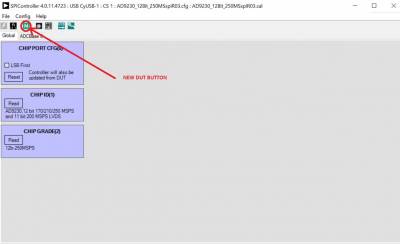
Figure 6. SPI Controller, New DUT Button
- Note that other settings can be changed in the Customer tab of the SPIController window. See the appropriate part data sheet, the AN-878 Application Note, High Speed ADC SPI Control Software, and the AN-877 Application Note, Interfacing to High Speed ADCs via SPI, for additional information on the available settings.

Figure 7. SPI Controller, ADCBase 0 Page
- Click the Run button in the VisualAnalog toolbar (see Figure 8).

Figure 8. Run Button (Encircled in Red) in VisualAnalog Toolbar, Collapsed Display


Adjusting the Amplitude of the Input Signal
The next step is to adjust the amplitude of the input signal for each channel as follows:
- Adjust the amplitude of the input signal so that the fundamental is at the desired level. Examine the Fund Power reading in the left panel of the VisualAnalog Graph - AD9230 FFT window (see Figure 9).

Figure 12. Graph Window of VisualAnalog
- Click the disk icon within the VisualAnalog Graph - AD9230 FFT window to save the performance plot data as a .csv formatted file. See Figure 10 for an example.


Figure 10. Typical FFT, AD9230
Troubleshooting Tips
If the FFT plot appears abnormal, do the following:
- If you see a normal noise floor when you disconnect the signal generator from the analog input, be sure you are not overdriving the ADC. Reduce the input level, if necessary.
- In VisualAnalog, click the Settings button in the Input Formatter block. Check that Number Format is set to correct encoding (offset binary by default). Repeat for the other channel.
If the FFT appears normal but the performance is poor, check the following:
- Make sure that an appropriate filter is used on the analog input.
- Make sure that the signal generators for the clock and the analog input are clean (low phase noise).
- Change the analog input frequency slightly if noncoherent sampling is being used.
- Make sure that the SPI configuration file matches the product being evaluated.
If the FFT window remains blank after Run is clicked, do the following:
- Make sure that the evaluation board is securely connected to the HSC-ADC-EVALCZ board.
- Make sure that the FPGA has been programmed by verifying that the DONE LED is illuminated on the HSC-ADC-EVALCZ board. If this LED is not illuminated, make sure that the U4 switch on the board is in the correct position for USB CONFIG.
- Make sure that the correct FPGA program was installed by clicking the Settings icon in the ADC Data Capture block in VisualAnalog. Then select the FPGA tab and verify that the proper FPGA bin file is selected for the part.
If VisualAnalog indicates that the FIFO Capture timed out, do the following:
- Make sure that all power and USB connections are secure.
- Confirm that a clock signal is present at the ADC sampling rate.
resources/eval/ad9230-250ebz.txt · Last modified: 03 Dec 2021 03:07 by Meriam Yuson-Aguila