 This version (24 Feb 2021 17:58) was approved by Umesh Jayamohan.The Previously approved version (24 Feb 2021 15:37) is available.
This is an old revision of the document!
This user guide describes additional modes and features available in the AD9082 Evaluation Board , AD9081 Evaluation Board, AD9986 Evaluation Board and AD9988 Evaluation Board. This guide explains the hardware and software setup needed to setup the AD9082, AD9081, AD9986 or AD9988 in the specified mode. The guide explains how a user can use the supplied hardware (AD9081-FMCA-EBZ, AD9082-FMCA-EBZ, AD9988-FMCB-EBZ or AD9986-FMCB-EBZ with ADS9-V2EBZ) and software (ACE) to setup the RF transceiver device in a mode that is not explained in the Evaluation Board User Guide.
The table below shows the various evaluation boards and their details.
| EVB Part # | Devices Supported | Power Delivery | Analog Front End Balun | Clock Input Balun | On-Board Crystal Oscillator Frequency |
|---|---|---|---|---|---|
| AD9081-FMCA-EBZ | AD9081 / AD9209 / AD9177 | via FMC connector: uModule and LDO | BALH-0009SMG | SMP + BAL-0416 | 100MHz |
| AD9082-FMCA-EBZ | AD9082 / AD9207 / AD9177 | via FMC connector: uModule and LDO | BALH-0009SMG | SMP + BAL-0416 | 100MHz |
| AD9988-FMCB-EBZ | AD9988 | External 12V using ADP5056 and LDO | TCM1-83X / LDB184G6 | SMA + NCR2-123+ | 122.88MHz |
| AD9986-FMCB-EBZ | AD9986 | External 12V using ADP5056 and LDO | TCM1-83X / LDB184G6 | SMA + NCR2-123+ | 122.88MHz |
A heat sink with integrated fan is shipped with the evaluation board for active cooling of the IC device. Note the power consumption of the IC device is dependent on its operation mode with some configurations consuming up to 13 W where the IC die temperature can approach or exceed its maximum specified operating range of 120 °C. For this reason, it is recommended that this heat sink shown in Figure 1 is installed before the evaluation process begins.
The installation steps are as follows:
The fan should start spinning once power is applied to the evaluation board. In the unlikely event that it does not spin, it has been found that the two screws used to secure the fan to the heatsink are too tight such that the fan blades cannot spin freely. Loosening the screws using a standard Phillips screwdriver often releases the fan blade allowing it to spin freely.
Additional information on this product called fanSink™ from Advanced Thermal Solutions can be found on the vendor’s website.
The following instructions allow the user to setup the MxFE chip in a single band 250MSPS I/Q data rate setup with direct RF sampling. The device is setup as shown below:
The evaluation board is setup to use the on-board HMC7044 and on-chip PLL to provide the DAC and ADC clocks. The HMC7044 also provides the clocks for the FPGA to setup the SERDES link correctly. Refer to the Evaluation board user guide (UG-1829) for more information on the hardware setup.
Open ACE and open the AD9081 plugin.
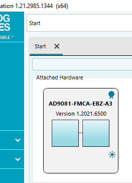 Double click on the AD9081 block to open the chip view
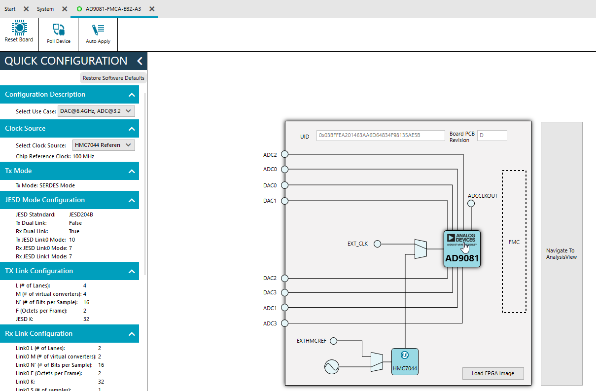 Configure the device Chip View's Quick Configuration section as shown in the figures below. The steps are numbered in sequence.


Hit Apply
Allow a few seconds for ACE and the ADS9v2 hardware to setup the AD9081. When the chip is configured correctly, the chip view will show a status readout as shown below.

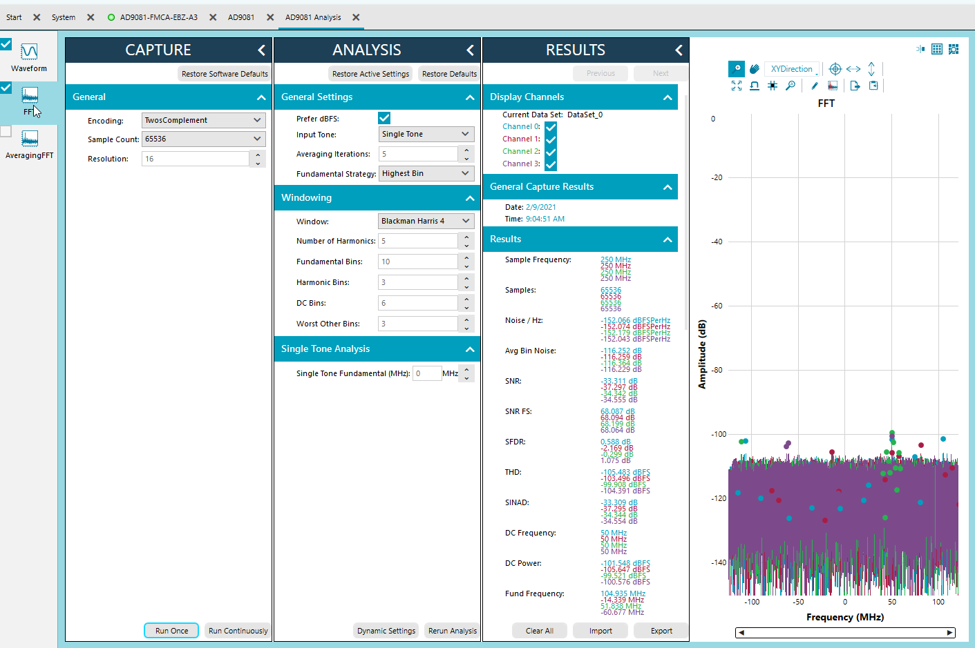
Click on “Proceed to Analysis” button to capture an FFT from the ADC. A no input FFT is shown below.
 Clicking on the “Update JESD Status” button in the chip view will output the FPGA's JESD204B link status. It will also readout the MxFE chip's junction temperature by polling the on-chip TMU
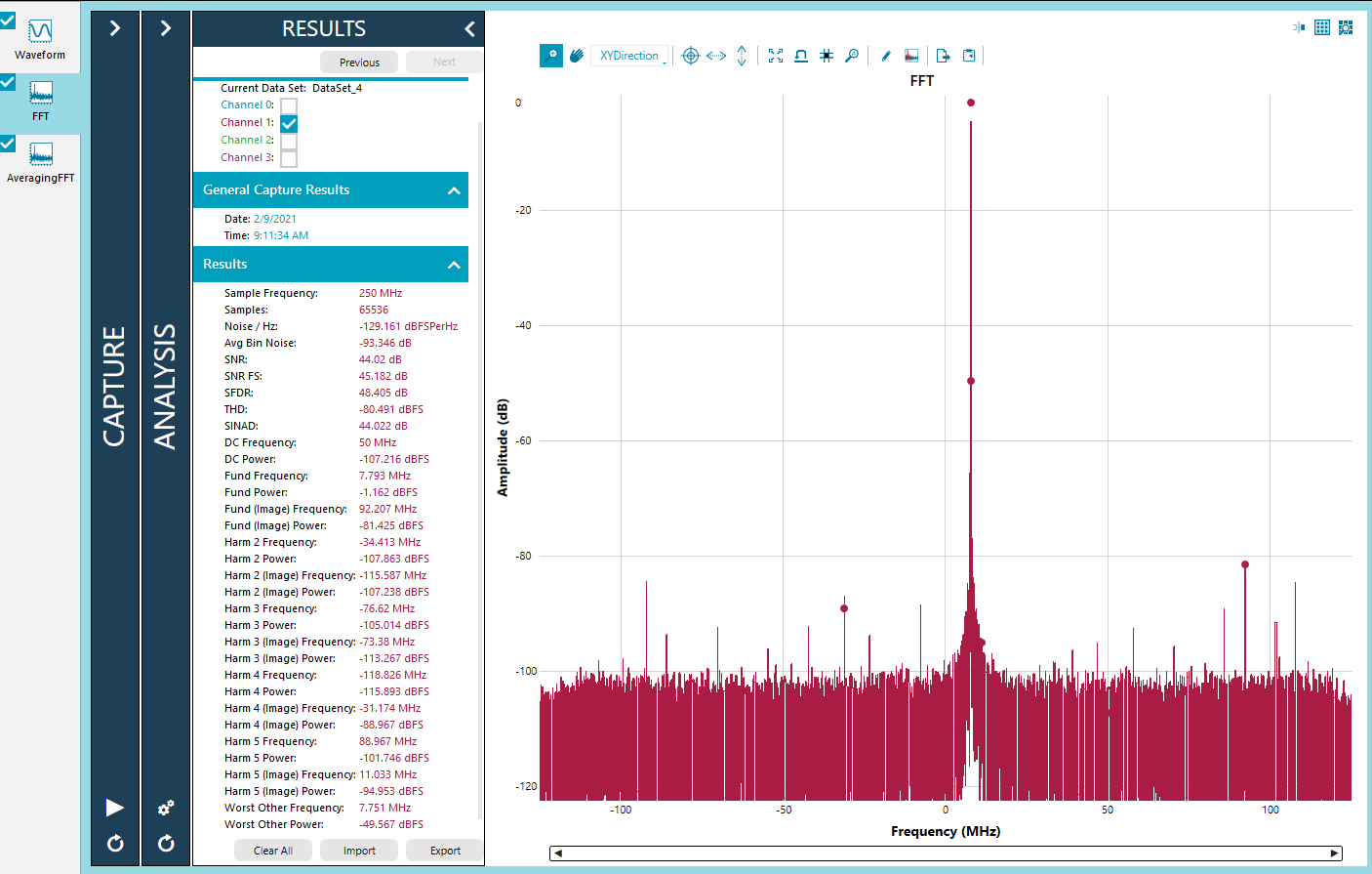
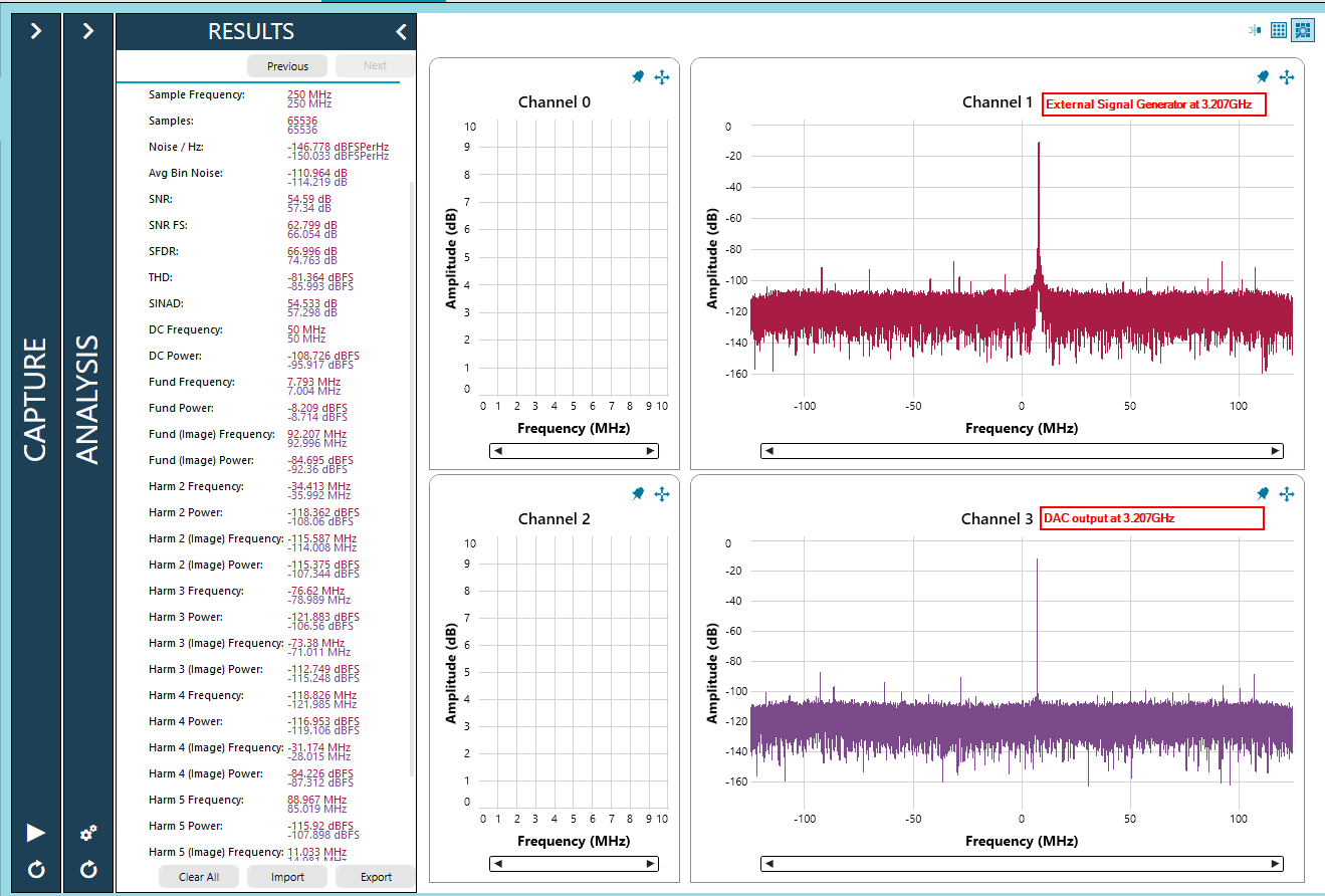
Connect a signal generator to any of the ADC inputs. Set the frequency to a 3.207GHz CW tone. The NCO is tuned to 3.2GHz. Set the amplitude to 5dBm for example. This will need to be adjusted based on cable and other RF losses. In the figure below, the signal generator output was set to 9.9dBm to get to ~-1.2dBFS fundamental power.
Open DPGDownloader Lite. Select a Single Tone waveform.
Configure the DPG Lite GUI as shown below. The steps necessary for the setup are enumerated.
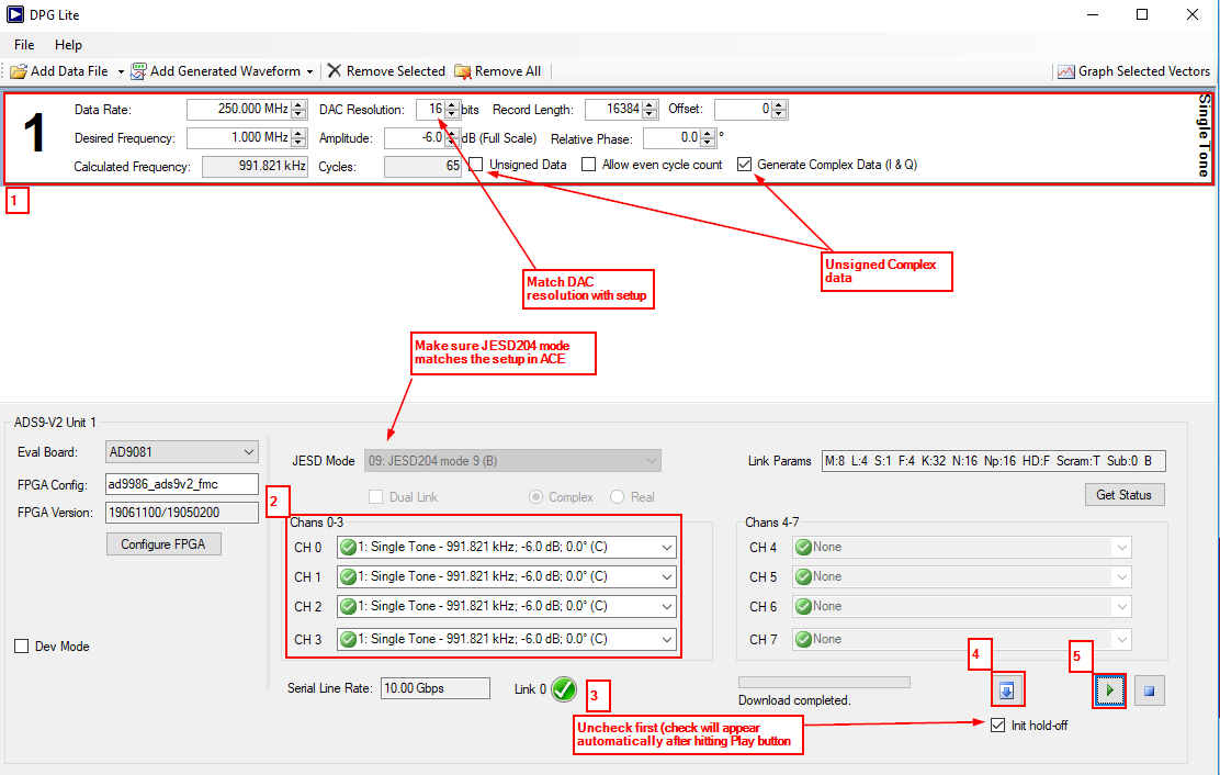 After enabling the DAC output by pressing the “Play” button in DPG Lite, use a SMA cable to connect DAC0 output to ADC3 input on the AD9081-FMCA-EBZ. Capture an FFT in ACE.
 Below is a screenshot of the ADC FFT with simultaneous capture of all four channels. ADC1 is sampling the signal generator output. ADC3 is sampling the DAC0 output.
The following instructions allow the user to setup the MxFE chip in a single band 1000MSPS I/Q data rate setup with direct RF sampling. The majority of the instructions are similar to the Narrowband use case. The device is setup as shown below:
Only showing the Quick configuration section with the appropriate inputs to setup the AD9081 in wideband mode.
Hit Apply
Allow a few seconds for ACE and the ADS9v2 hardware to setup the AD9081.
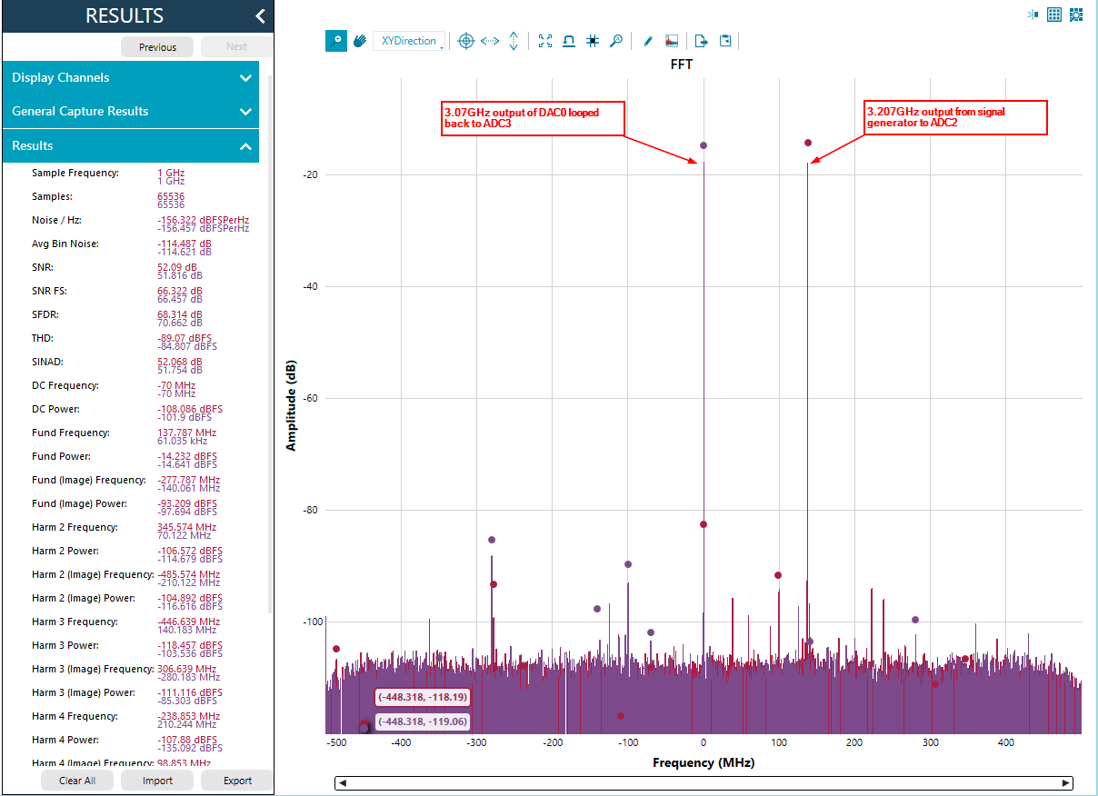
Connect a signal generator to any of the ADC inputs. Set the frequency to a 3.207GHz CW tone.
Click on “Proceed to Analysis” button to capture an FFT from the ADC.
The AD9081/AD9988 and AD9082/AD9986 have flexible digital signal processing (DSP) that allows it to act as a 4T4R (4 transmit and 4 receive) transceiver for multiband radios. Below is an example showing the AD9081/AD9988 in a multiband setup, where the device processes LTE bands 1 and 4. The band details are shown below
| Band | Duplex Mode | f(MHz) | Uplink (MHz) | Downlink (MHz) |
|---|---|---|---|---|
| 1 | FDD | 2100 | 1920 - 1980 | 2110 - 2170 |
| 4 | FDD | 1700 | 1710 - 1785 | 1805 - 1880 |
For optimal performance of the AD9081/AD9988 in a direct RF conversion mode, it is essential to have a good frequency plan. In this example, a DAC sample rate (fDAC) of 4.9152GHz and an ADC sample rate (fADC) of 2.4576GHz. The frequency plan of the receive path (ADC) is shown below.
To support the dual band operation, the AD9081/AD9988 will need to be configured as shown below. Please note that the AD9081-FMCA-EBZ and AD9988-FMCB-EBZ have different standard crystal oscillators. The AD9988-FMCA-EBZ has an on-board 122.88MHz crystal, and therefore can be configured using ACE, on-board HMC7044, and on-chip PLL. For the example below, the AD9081-FMCA-EBZ was modified to use a direct external clock, bypassing the HMC7044 and on-chip PLL. Refer to the Evaluation Board User Guide (UG-1829) for more details.
Follow the steps below to configure AD9081/AD9988 in the ACE GUI. The Quick configuration setup summary is shown in the screenshots below. Please note that in this example, a direct external clock was used. Please refer to UG-1829 for details on how to run the evaluation board using an external clock source.
Below is an FFT of the ADC sampling a 1.7325GHZ CW tone
and the ADC sampling a 1.95GHZ CW tone
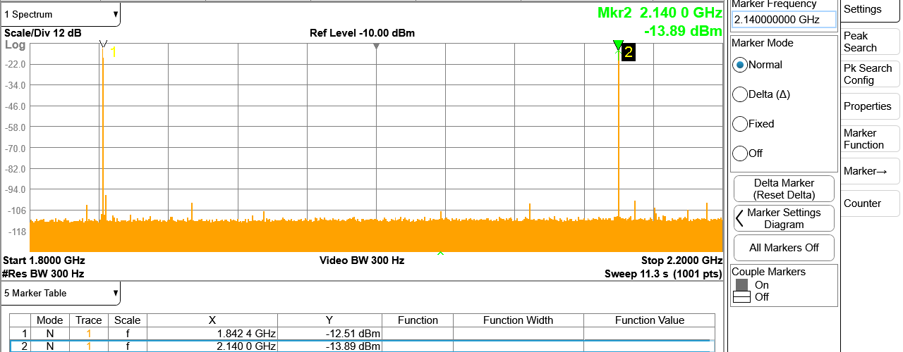
Below is the spectrum of the DAC output two tones representing the center frequencies of the two bands.
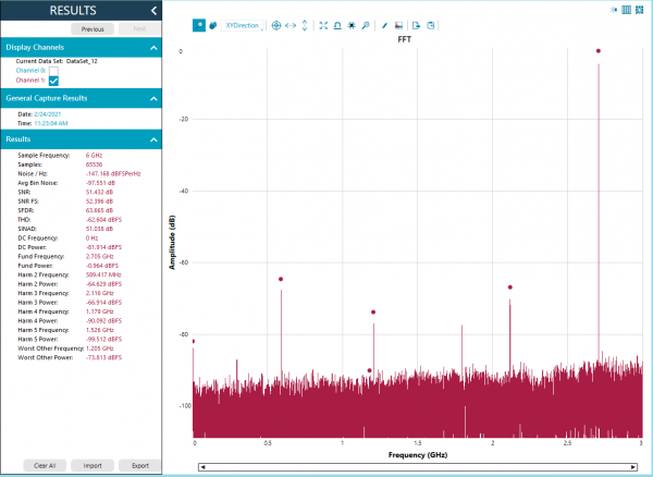
The AD9081/AD9988/AD9082/AD9986 are highly integrated direct RF transceivers. Hence, the performance of the ADC may vary based on the device setup. For example, if the AD9082-FMCA-EBZ was setup to run in a transceiver mode (with DACs ON), and receive only mode (ADC only), there will be a noticeable difference in the ADC's noise performance. See below:

This section of the user guide talks about how to run the MATLAB code for the BPF compensation filter design and use the coefficients generated from it to load the PFILT on AD9082-FMCA-EBZ board using ACE plug-in. The same technique can be applied to the other evaluation boards listed above, as well. In this document we are considering that you have a working set up of the AD9082-FMCA-EBZ with following instructions from UG-1829 as listed under the Documents needed section. Please refer to UG-1829 for hardware needed, how to load ACE software and the required plug-in for using the AD9082-FMCA-EBZ.
Where to start PFILT design – to equalize the response using the PFILT. How to download the MATLAB model for PFILT? For documentation on the MATLAB support refer to this Wiki page: https://wiki.analog.com/resources/tools-software/hsx-toolbox Please download the entire toolbox with the link off the main README: https://github.com/analogdevicesinc/HighSpeedConverterToolbox/blob/master/README.md Then all the helper functions are on path. You can download the toolbox directly within MATLAB through Addon Explorer or grab the source from GitHub. This is documented here: https://wiki.analog.com/resources/tools-software/hsx-toolbox. This MATLAB support is provided through ADI’s High Speed Converter Toolbox. Click on this link below on GitHub https://github.com/analogdevicesinc/HighSpeedConverterToolboxand use the green button code as shown below to download the Compensation Filter folder under hsx_examples/mxfe_sim/
 Figure 2: HighSpeedConverterToolBox under GitHub
Under the Compensation Filter Folder you should see the following:
 Figure 3: Compensation Filter Folder view under HighSpeedConverterToolBox
This document uses the MxFEADCCompensationFilterDesign_BPF.m MATLAB code.
 Figure 4: BPF MATLAB code view under MATLAB
You can either use the Run on the Editor Tab.Or Run individual sections on the Editor Tab.
The MATLAB code uses the input response of the ADC in the file “MXFE_ADC_Response” When you run the MATLAB code for the BPF you will get this output response below, which we are interested in. We define the Pass Band and the 2 Stop Bands for this ADC response. We then generate the target response similar to the red trace in the figure. This is the filter that is generated. It is the one in red which is the magnitude compensation filter. The composite response is the one in yellow. This is for 192 tap BPF filter per channel.
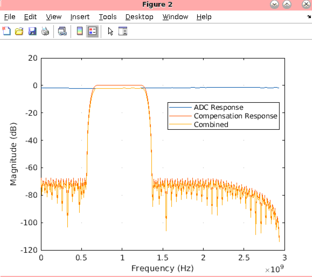 Figure 5: BPF Compensation Filter Response
This is the output response that we try to replicate on the bench measurements using the AD9082-FMCB-EBZ. The MATLAB code also generated this figure below which defines the target response for the 2 Stop bands and Pass bands.
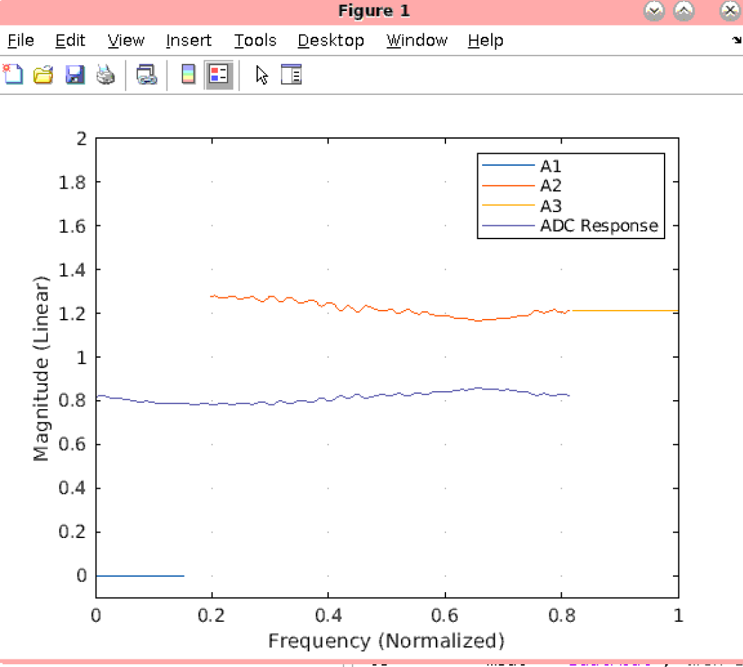 Figure 6: Target Responses for the BPF Compensation Filter design
When you type on the command window, “xt”, you will get the coefficient values as shown below: It generates coefficients to load into PFIR on MxFE using the HW AD9082-FMCB-EBZ. The coefficient format generated in MATLAB is in decimal format.
It needs to be converted to 2’s complement and then to Hex Format prior to loading it to the PFILT on AD9082-FMC-EBZ hardware using ACE plug-in
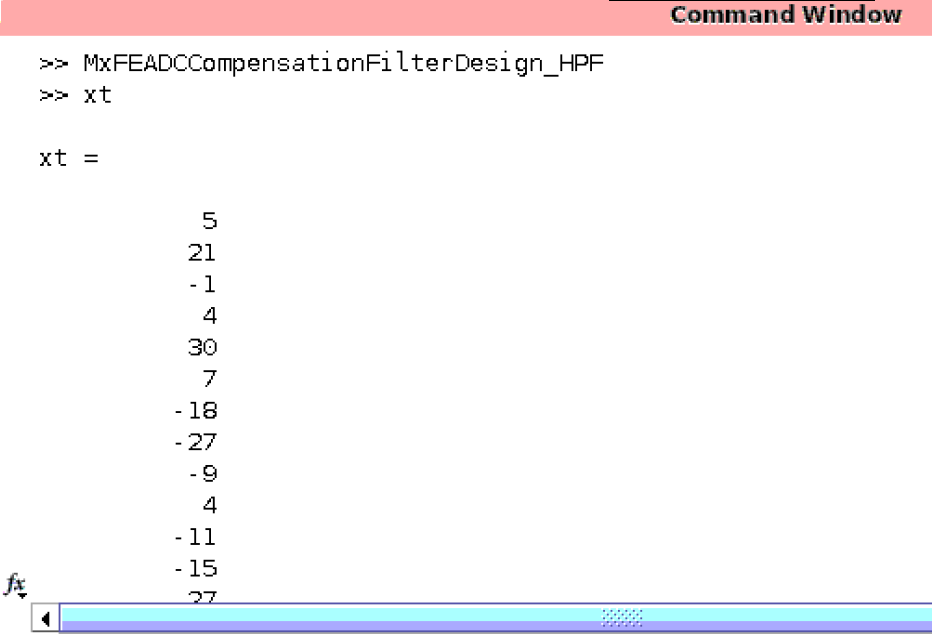 Figure 7: Coefficient values in Decimal format generated from the MATLAB code for the BPF
The coefficient /taps are generated from MATLAB. These are in decimal format. Prior to loading into ACE, these need to be converted to 2’s complement first and then to Hex format. Example of how the coefficient file looks like after converting into Hex. It is a text file and below is an excerpt from a coefficient file for a bandpass, 192 tap filter.
 Figure 8: Excerpt from a Coefficient file for PFILT loading
In this document we are considering that you have a working set up of the AD9082-FMCB-EBZ with following instructions from UG-1829 as listed under the Documents needed section. Once you have a working set up of the AD9082-FMCB-EBZ, please use the last ADC Full Bandwidth condition shown under Table 2 of Page 11 of the UG-1829.
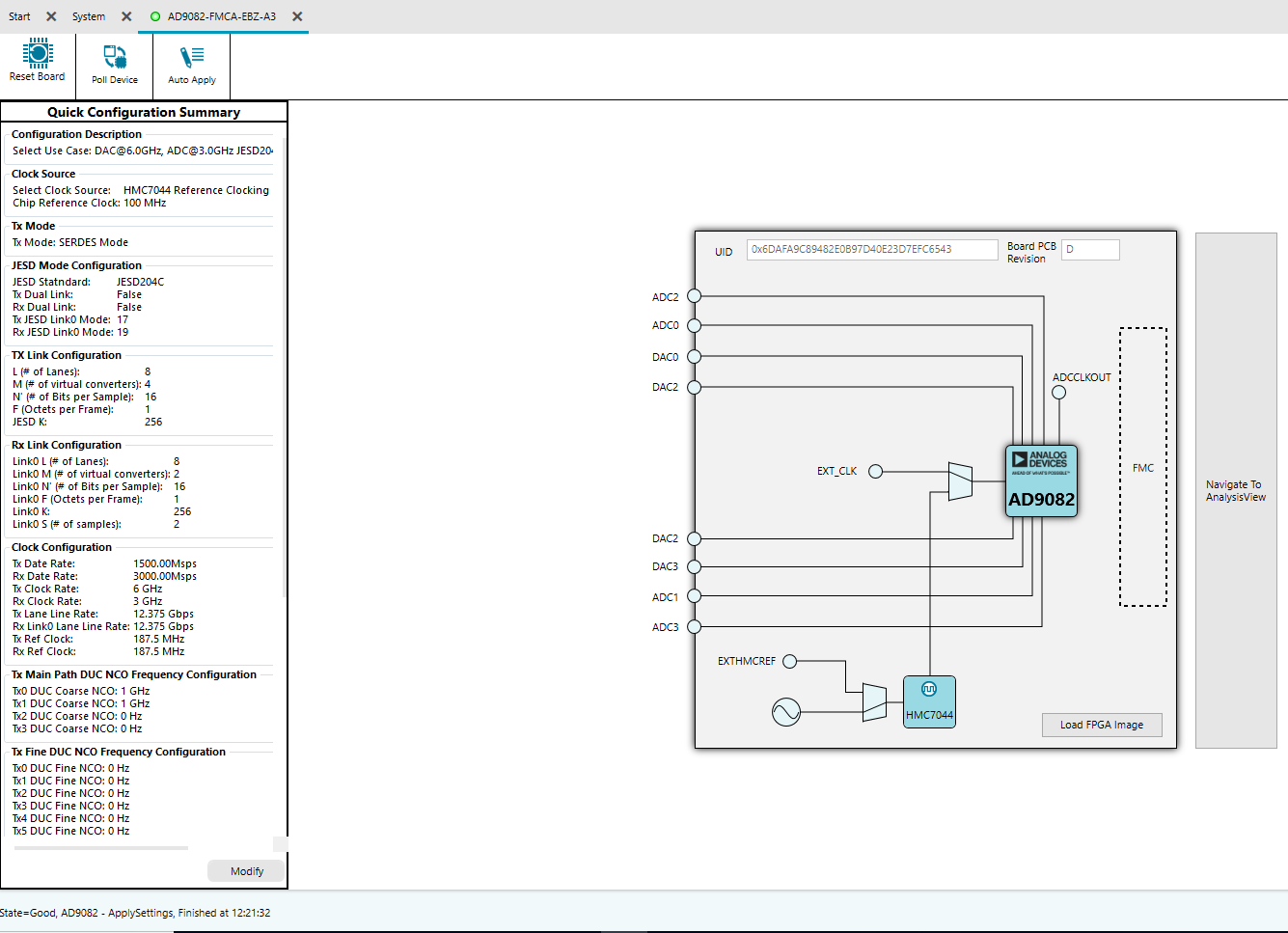 Figure 9: Board View of selected Full Bandwidth ADC Use Case
You can check the FFT response of the signal without PFILT:
 Figure 10: FFT of the signal @0.5GHz to ADC input, without PFILT
How to load the generated coefficients by MATLAB code in the ACE Tool? 1.Design Band pass filter in MATLAB PFILT tool to equalize the ADC input: For a 192 tap single real mode PFILT: Use the following settings under Quick Configuration tool in Chip view for AD9082 board. You get to the chip view by click on the highlighted box in green in the figure below
 Figure 11: AD9082 Board view under ACE Plug-in
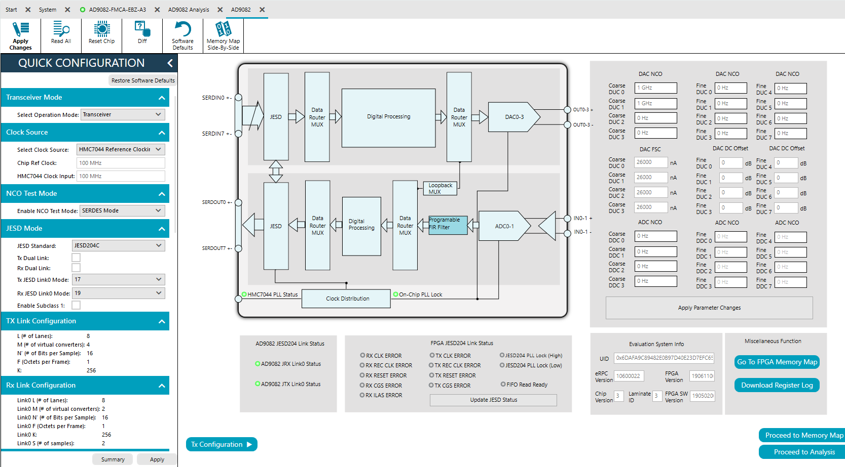 Figure 12: AD9082 Chip view under ACE Plug-in
Configuring the Programmable Filter in ACE: 1.Click the programmable filter block in chip as highlighted in the picture below.
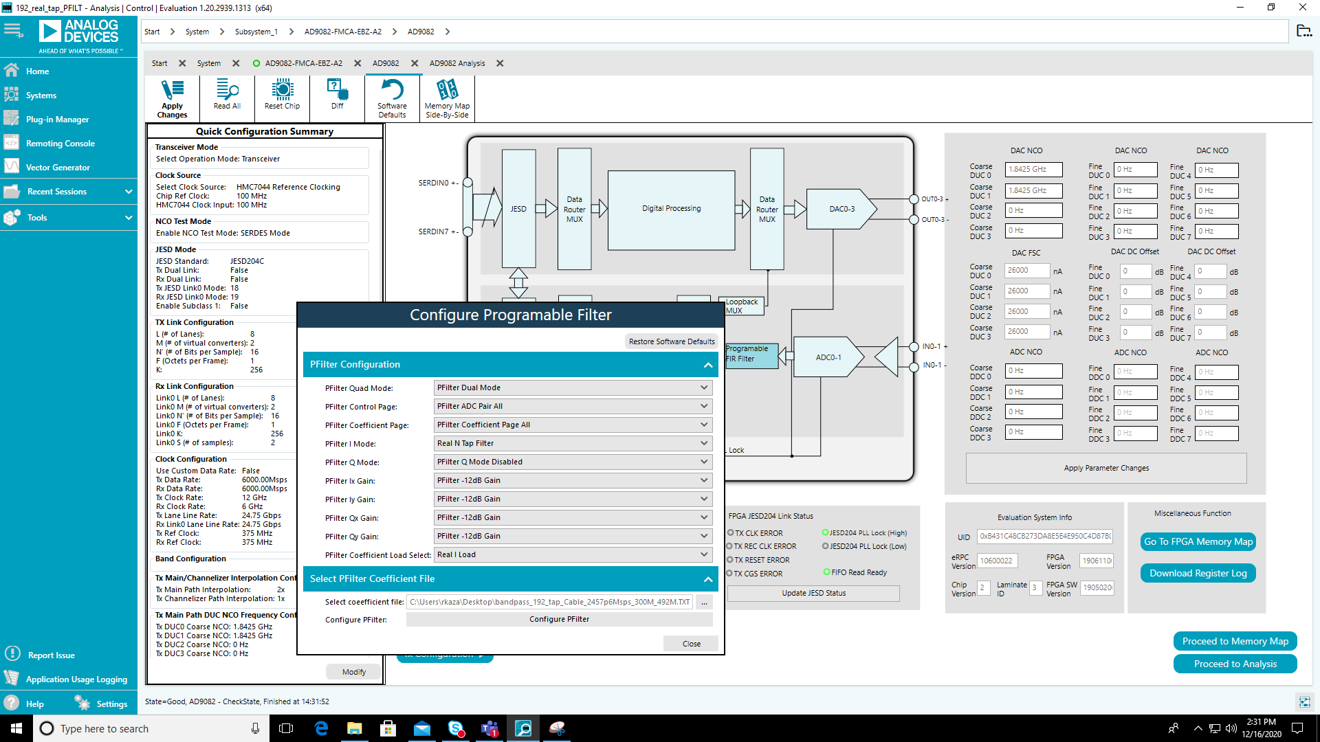 Figure 13: Programmable Filter Configuration Pop-up Window
2.The settings shown in the Programmable filter configuration shows for AD9082 TxFE. As, TxFE only has two ADCs. If it AD9081, under PFILT Quad mode selection we need to choose PFilter Quad mode. We have selected Real N Tap Filter for PFILT I mode and PFILT Q Mode is disabled.
3.Depending on whether, PFilter I Mode or PFilter Q Mode is selected, then the PFILTER Coefficient Load select should be Real I Load or Real Q load.
4.Under Analysis window, Channel 0 is I data, Channel 1 is Q data.
5.Under select the PFilter coefficient file, load the coefficient file. The coefficients needs to be in Hex Format when we upload them in ACE. So we convert the coefficients generated from MATLAB from Decimal 2’s complement Hex Format before loading into ACE.
6.Once the coefficient file is loaded, click the Configure Filter Block under the chip view. Please note that it takes several seconds to complete loading the coefficients into the PFILT block.
7.Now proceed to Analysis by click at the “Proceed to Analysis” button at the bottom of the chip view page.
8.Below is the FFT plot at sampling frequency of 3Gsps and input to the ADC is 0.5GHz.
Showing Channel 0 which I Mode.
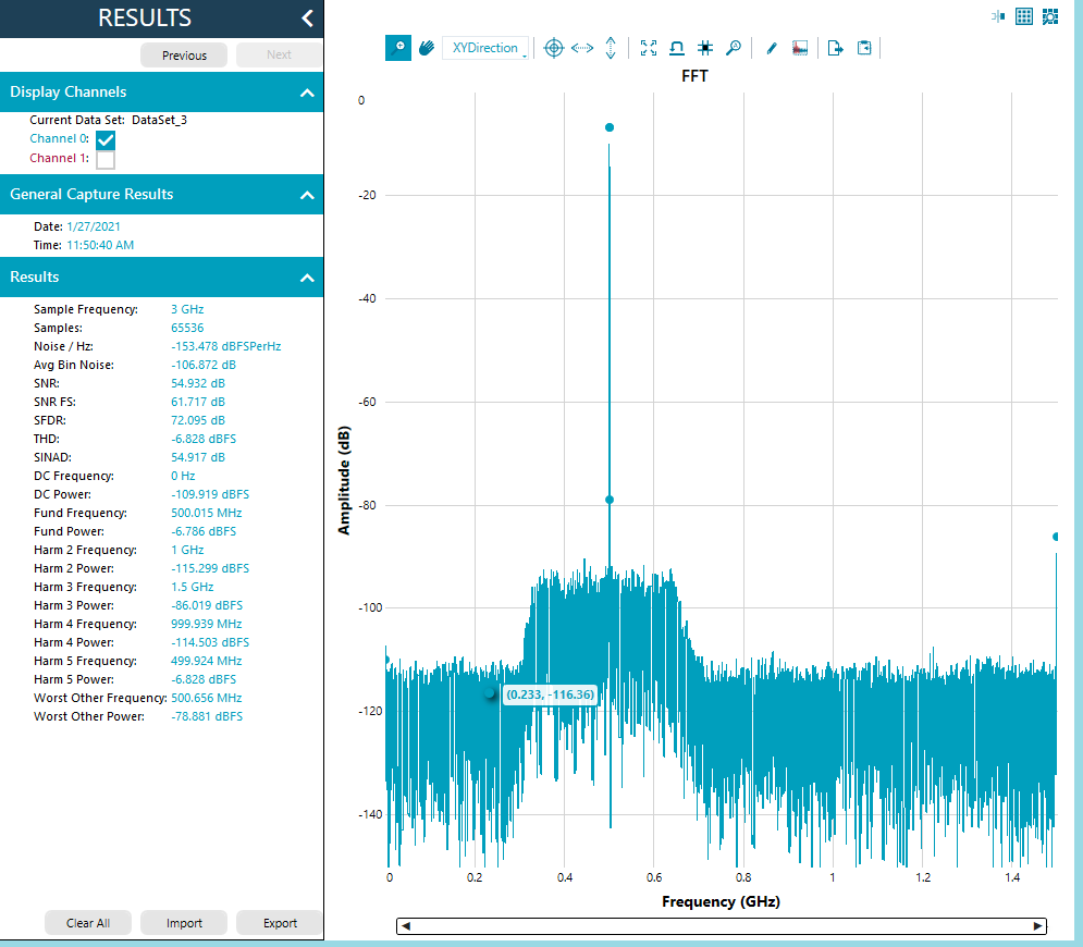 Figure 15: FFT plot at sampling frequency of 3Gsps
This FFT plot correlates to the MATLAB compensation filter response shown in Figure 5.
If you select the Channel 1 which is Q channel and as Q mode is disabled for the selected 192 tap single real PFilter configuration. So no signal seen on the FFT plot below.
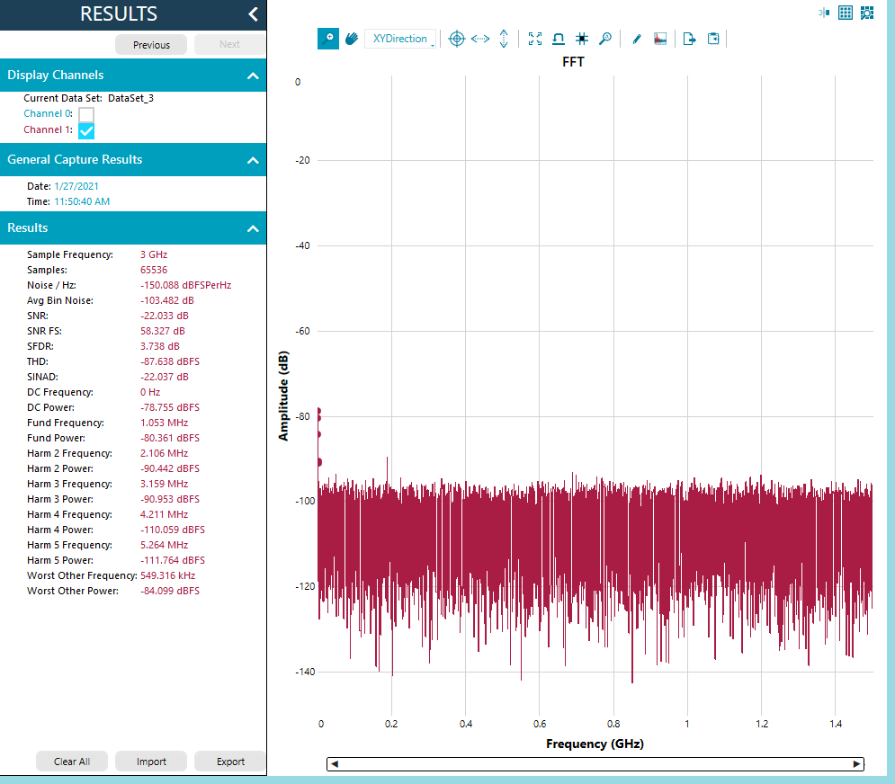 Figure 16: FFT plot Channel 1 which is Q channel with Q mode Disabled under PFILT Configuration Tool
9.Under the configuration window for PFILT, if you select the PFILT Q mode and disable the PFILT I mode. Then the FFT plot for Channel 1 will be showing the signal transmission as below:
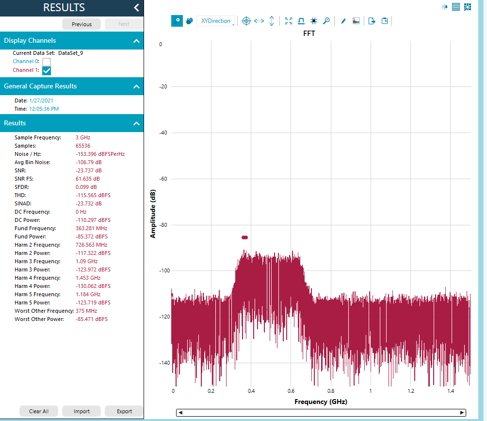 Figure 17: FFT plot Channel 1 which is Q channel with Q mode Enabled under PFILT Configuration Tool.
Evaluation Board is not Functioning Properly
ACE is slow to capture data and setup the board
Unable to capture data after device is setup
In some instances, the user may be unable to capture data from the FPGA. This is characterized by no capture via ACE, or a “configure channel failed” error in ACE. In either case, only four of the six LEDs on the FPGA board will be lit (see figure below).
If this happens, and the setup is using an external direct clock to the chip, ensure that the instrumentation is setup as explained in the evaluation board user guide UG-1829. Ensure the correct clock and refclock frequencies are set. Check the connections to the board to make sure they are snug. If the problem persists, open DPG Lite and download a tone. After this step, a successful data capture will show all the LEDs lit. See figure below.
HMC7044 Configuration Error
When operating with the on-board clocking and on-chip PLL mode, the user can get a “HMC7044 Configuration Error” in the ACE setup.
If this happens, ensure the correct modes are selected to setup the chip. Please note that not all modes that are listed in the UG-1578, device user guide, are supported by the evaluation board hardware using the on-board HMC7044 clock and on-chip PLL. This is because the HMC7044 derives the reference from a 100MHz crystal oscillator if using the FMCA version, or 122.88MHz crystal oscillator if using the FMCB version of the evaluation board.
If this use case is required, the best approach is to switch to using the direct external clock. This bypasses the HMC7044 setup and the user is not limited to the setup options provided only by the combination of on-board crystal oscillator and the HMC7044 setup.