


This version is outdated by a newer approved version. This version (04 Sep 2019 13:20) was approved by Donal O''Sullivan.The Previously approved version (03 Sep 2019 15:17) is available.
This version (04 Sep 2019 13:20) was approved by Donal O''Sullivan.The Previously approved version (03 Sep 2019 15:17) is available.This is an old revision of the document!
AD5758 + ADP1031 Eight Channel Analog Output Module
Using the Demo Board
Before proceeding, please ensure you have the DEMO_AD5758-AO8Z Demo software installed on your PC or Laptop and that the latest version of the firmware has been uploaded to the board. Instructions on how to complete these steps can be found earlier in this guide in the Software Details section.

Figure 1 - DEMO-AD5758-AO8Z Setup
Connecting the Board
- Remove Jumpers P4 & P5
- Connect the power supplies as show in Figure 1. The field power supply should be capable of supplying at least 300 mA @ 24 V. The system supply needs to only supply about 20 mA (max) @ 24 V
- Alternatively, if only one power supply is available, then P4 & P5 jumpers can be left in place and a single field supply used.
If either P4 and/or P5 jumpers are inserted, then there will be no isolation between the system domain and the field power domain.
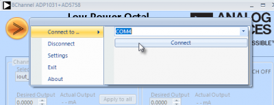
- Connect a USB cable from your PC or laptop to the USB port on the demo board.
- Start the DEMO-AD5758-AO8Z GUI Software and select the correct COM port, then click [Connect]
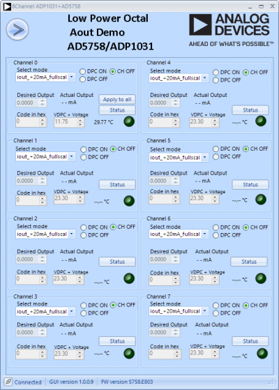
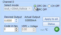
- The GUI display should resemble the following image.


DPC ON vs. DPC OFF Demonstration
- Quiescent Current should be approximately:-
- IFIELD = 26 mA ± 5 mA
- ISYSTEM = 3 mA ± 1 mA
- Connect a 1 Ω resistors to each of eight channel headers (CH0 to CH7].
Resistor values between 0 Ω and 1 kΩ can be used. However, lower values provide a more challenging load and demonstrate the DPC mode power savings better.
- Turn on Channel 0 by clicking the DPC OFF radio button. This turns on the channel but leaves DPC mode disabled by fixing the output of the DPC buck (and thus the power supply to the buffer) to 23.3 V

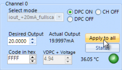
- Set Desired Output to 20 mA and click Apply to all. This will set the remaining channels to the same state as channel 0. i.e. 20 mA output, DPC OFF.
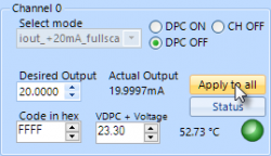
Observe that VDPC+ is fixed at 23.3 V even though the buffer output is at 0 V.
- IFIELD should now be around 207 mA ± 10 mA (~5 W). ISYSTEM should be relatively unchanged.
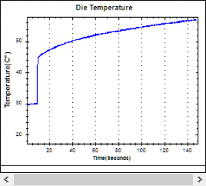
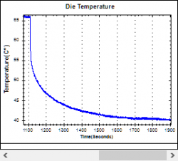
- Click the Status button of any channel to see a graph of the internal die temperature rise of the AD5758. Notice how the temperature rises rapidly when DPC is disabled.
When DPC mode is turned off, the DPC buck is programmed to output a fixed voltage of 23.3 V. Because the load resistance is low (1 Ω), there is a large voltage drop across the AD5758 output buffer. There is 23.3V X 20mA = 466mW of power dissipated in the output buffer plus an additional 47 mW dissipation in the DPC buck regulator
(466 mW X (1-η)). Which translates to 513 mW of dissipation per channel in the module. - Now select CH0 DPC ON
- Click “Apply to all”.
Notice how VDPC+ is now at its minimum value of approximately 4.95 V and the die temperature begins to drop rapidly as DPC power saving take effect.
When DPC mode is turned on, a high efficiency (η = 0.9) buck converter reduces the supply to the buffer to 2.5 V above the required output voltage or 4.95 V - whichever is higher, so there is now a small voltage drop of only 4.95 V across the AD5758 output buffer1. This translates to 4.95V X 20mA = 99mW plus 99 mW X (1 - η) = 10 mW of heat dissipation in the output buffer of the AD5758. This is a power saving of 404 mW per channel.
1 If VIOUT > 2.5 V, then the the DPC buck tracks the output to maintain a fixed 2.5 V headroom. - IFIELD should now be around 72 mA ± 5 mA (~ 1.7 W). ISYSTEM should be unchanged.


Related Resources
Navigation
resources/demo/reference-designs/demo-ad5758-ao8z/demonstration_guide.1567595992.txt.gz · Last modified: 04 Sep 2019 13:19 by Donal O''Sullivan