


This version is outdated by a newer approved version. This version (09 Apr 2013 16:06) is a draft.
Approvals: 0/1The Previously approved version (12 Feb 2013 16:56) is available.
This version (09 Apr 2013 16:06) is a draft.Approvals: 0/1The Previously approved version (12 Feb 2013 16:56) is available.
This is an old revision of the document!
Table of Contents
AD5781/AD5791 Quick Start Guide
Single, 18-/20-Bit, Voltage Output DACs, SPI Interface
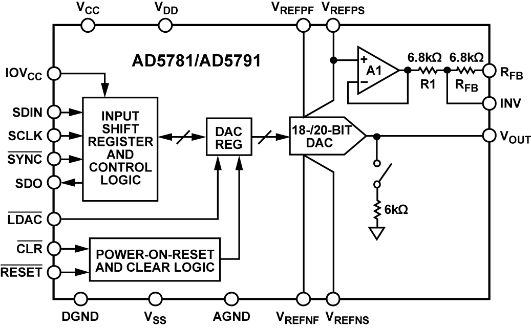
Figure 1. Functional Block Diagram
Features
- High relative accuracy (INL): ±0.5 LSB maximum (18-bit AD5781)
- 1ppm resolution, 1ppm INL (20-bit AD5791)
- 7.5 nV/√Hz output noise spectral density
- 0.19 LSB long-term linearity error stability (20-bit AD5791)
- <0.05 ppm/°C temperature drift
- 1 μs output voltage settling time
- 1.4 nV-sec midscale glitch impulse
- Operating temperature range: −40°C to +125°C
- 20-lead TSSOP package
- Wide power supply range up to ±16.5 V
- 35 MHz Schmitt triggered digital interface
- 1.8 V compatible digital interface
Pin Configurations
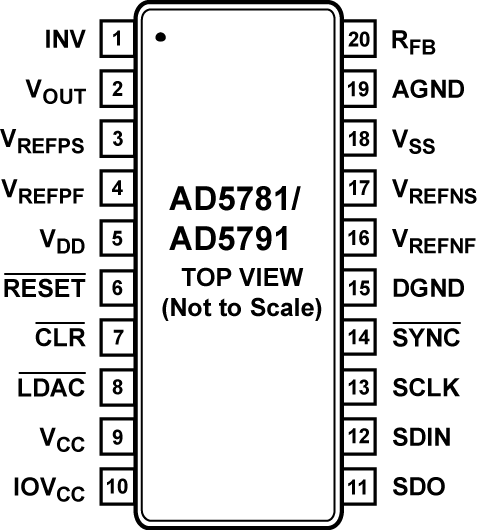
Figure 2. 24-Lead LFCSP
Table 1. Function Descriptions for Quick Start
| Mnemonic | Description |
|---|---|
| INV | Inverting Input Connection for External Amplifier. |
| VOUT | Analog output voltage. |
| VREFPS | Positive Reference Sense Voltage Input. Connect a voltage in the range of 5V to VDD - 2.5V. |
| VREFPF | Positive Reference Force Voltage Input. Connect a voltage in the range of 5V to VDD - 2.5V. |
| VDD | Positive Analog Supply Connection. Connect a voltage in the range of 7.5V to 16.5V. VDD must be decoupled to AGND. |
| Active Low Reset. Asserting this pin returns the DAC to its power-on status. | |
| Active Low Input. Asserting this pin sets the DAC register to a user defined value and updates the DAC output. | |
| Active Low Load DAC Logic Input. This is used to update the DAC register and, consequently, the analog output. | |
| VCC | Digital Supply. Connect a voltage in the range of 2.7V to 5.5V. VCC should be decoupled to DGND. |
| IOVCC | Digital Interface Supply. Voltage range is from 1.71V to 5.5V. |
| SDO | Serial Data Output. |
| SDIN | Serial Data Input. |
| SCLK | Serial Clock Input. Data can be transferred at clock rates of up to 35 MHz. |
| Active Low Digital Interface Synchronization Input Pin. This is the frame synchronization signal for the input data. | |
| DGND | Ground Reference Pin for Digital Circuitry. |
| VREFNF | Negative Reference Force Voltage Input. Connect a voltage in the range of VSS + 2.5V to 0V. |
| VREFNS | Negative Reference Sense Voltage Input. Connect a voltage in the range of VSS + 2.5V to 0V. |
| VSS | Negative Analog Supply Connection. Connect a voltage in the range of -16.5V to -2.5V. VSS must be decoupled to AGND. |
| AGND | Ground Reference Pin for Digital Circuitry. |
| RFB | Feedback Connection for External Amplifier. |
Hardware Control Pins Truth Table
Table 2. Hardware Control Pins Truth Table
| /LDAC | /CLR | /RESET | Function |
|---|---|---|---|
| X1 | X1 | 0 | DAC in reset mode. The device cannot be programmed. |
| X1 | X1 | ⇑2 | DAC is turned to its power-on state. All registers are set to their default values. |
| 0 | 0 | 1 | DAC register loaded with the clearcode register value and output set accordingly. |
| 0 | 1 | 1 | Output set according to the DAC register value. |
| 1 | 0 | 1 | DAC register loaded with the clearcode register value and output set accordingly. |
| ⇓3 | 1 | 1 | Output set according to the DAC register value. |
| ⇓3 | 0 | 1 | Output remains at the clearcode register value. |
| ⇑2 | 1 | 1 | Output remains set according to the DAC register value. |
| ⇑2 | 0 | 1 | Output remains at the clearcode register value. |
| 1 | ⇓3 | 1 | DAC register loaded with the clearcode register value and output set accordingly. |
| 0 | ⇓3 | 1 | DAC register loaded with the clearcode register value and output set accordingly. |
| 1 | ⇑2 | 1 | Output remains at the clearcode register value. |
| 0 | ⇑2 | 1 | Output set according to the DAC register value. |
1 X is don't care.
2 ⇑ is rising edge.
3 ⇓ is falling edge.
Shift Register Contents

Figure 3. Shift Register Contents (AD5791)
Table 3. Register Address Definitions
| Read/Write | Register Address | |||
|---|---|---|---|---|
| R/W | C2 | C1 | C0 | Description |
| X | 0 | 0 | 0 | No operation |
| 0 | 0 | 0 | 1 | Write to the DAC Register |
| 0 | 0 | 1 | 0 | Write to the Control Register |
| 0 | 0 | 1 | 1 | Write to the Clearcode Register |
| 0 | 1 | 0 | 0 | Write to the Software Control Register |
| 1 | 0 | 0 | 1 | Read from the DAC Register |
| 1 | 0 | 1 | 0 | Read from the Control Register |
| 1 | 0 | 1 | 1 | Read from the Clearcode Register |
Control Register
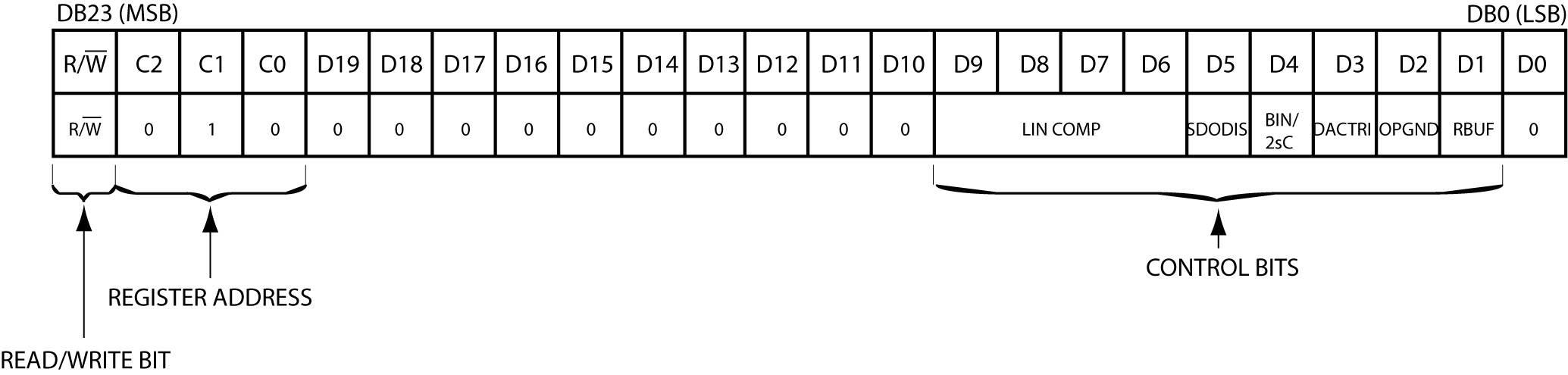
Figure 4. Control Register (AD5791)
Table 4. Control Register Functions
| Bit Name | Description |
|---|---|
| RBUF | Output amplifier configuration control. “0”: Internal amplifier powered up. “1”: (default) Internal amplifier powered down. |
| OPGND | Output ground clamp control. “0”: DAC output clamp to ground removed and DAC placed in normal mode. “1”: (default) DAC output clamped to ground and DAC placed in tristate mode. |
| DACTRI | DAC tristate control. “0”: DAC in normal operating mode. “1”: (default) DAC in tristate mode. |
| BIN/2sC | DAC register coding selection. “0”: (default) DAC register uses twos complement coding. “1”: DAC register uses offset binary coding. |
| SDODIS | SDO pin enable/disable control. “0”: (default) SDO pin enabled. “1”: SDO pin disabled (tristate). |
| LIN COMP | Linearity error compensation for varying reference input spans. “0000”: (default) reference input span up to 10 V. “1001”: Reference input span between 10 V and 12 V. “1010”: Reference input span between 12 V and 16 V. “1011”: Reference input span between 16 V and 19 V. “1100”: Reference input span between 19 V and 20 V. |
| R/ | Read/write select bit. “0”: (AD5790) addressed for a write operation. “1”: (AD5790) addressed for a read operation. |
Software Control Register

Figure 5. Software Control Register (AD5791)
Table 5. Software Control Register Functions
| Bit Name | Description |
|---|---|
| LDAC2 | Setting this bit to 1 updates the DAC register and consequently the DAC output. |
| CLR1 | Setting this bit to 1 sets the DAC register to a user defined value and updates the DAC output. |
| RESET | Setting this bit to 1 returns the (AD5790) to its power-on state. |
1 The CLR function has no effect when the pin is low. Refer to the Hardware Control Pins Truth Table for further detail.
2 The LDAC function has no effect when the pin is low. Refer to the Hardware Control Pins Truth Table for further detail.
Transfer Function
where:
VREFN is the negative voltage applied at the VREFN input pin.
VREFP is the positive voltage applied at the VREFP input pin.
D is the decimal equivalent.
N is the number of bits.
Example 1: Initializing and writing to the DAC Register
Initializing the DAC
To initialize the part,
- Remove the DAC output clamp to ground and place the DAC in normal operating mode (OPGND = “0”, DACTRI = “0”).
- As this initializing is a write to the part, R/W bit should be a logic “0”.
- To write in binary coding select BIN/2sC = “1”.
- Keep the default mode for RBUF, SDODIS and LIN COMP:
- The internal amplifier powered down (RBUF = “1”)
- The SDO pin enabled for future readings from the part (SDODIS = “0”)
- Linearity error compensation for a reference input span up to 10V. (LIN COMP = “0000”)
Write the following over the serial interface: 0010 0000 0000 0000 0001 0010 (Read/Write bit, three register address bits, 20 data bits).
To write in binary coding select BIN/2sC = “1”.
The default coding is the offset binary, the same 24-bit data will impact in a different way depending on the coding selected. The user will need to ensure the coding used by writing to the control register or reading back from it.
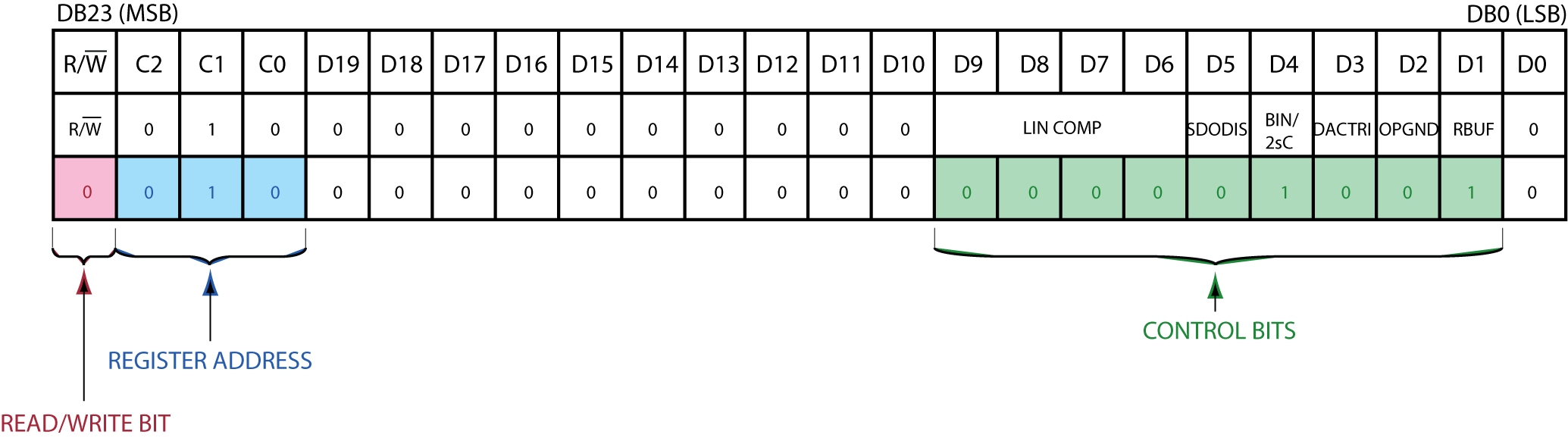
Figure 6. Initializing the part
Writing to the DAC Register
To write a midscale code to the DAC register, select the write option from the read/write bit (R/W = “0”), the correspondent register address (C2C1C0 = “001”) and the data bits for a midscale code.
The 24-bit data to write over the serial interface is:
18-bit AD5781: 0001 1000 0000 0000 0000 00XX
20-bit AD5791: 0001 1000 0000 0000 0000 0000
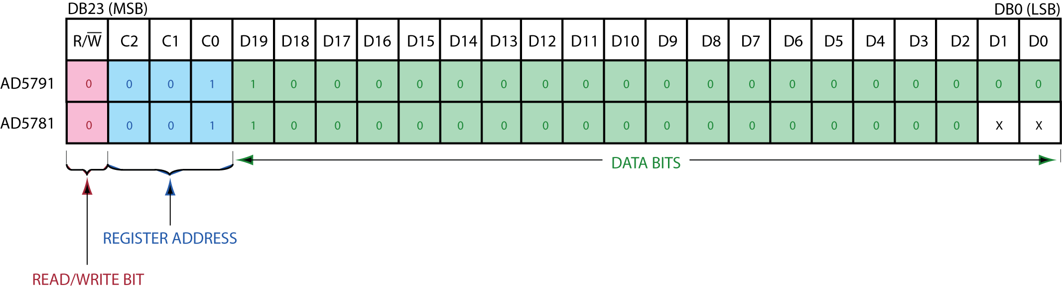
Figure 7. Write to the DAC Register)
Example 2: Clear the DAC to a defined value
Writing to the Clearcode Register
To define the value at which the DAC output is set when the CLR pin or CLR bit in the software control register is asserted, write the desired code to the clearcode register.
For a full scale clear code, write the following over the serial interface:
18-bit AD5781: 0011 1111 1111 1111 1111 11XX
20-bit AD5791: 0011 1111 1111 1111 1111 1111

Figure 8. Write Full Scale code to the Clearcode Register
Writting to the Software Control Register
To set the DAC register to a user defined value and update the DAC output set the CLR bit to a logic “1”.
Write the following over the serial interface: 0100 0000 0000 0000 0000 0010
The user should see the DAC output value change to full scale code.
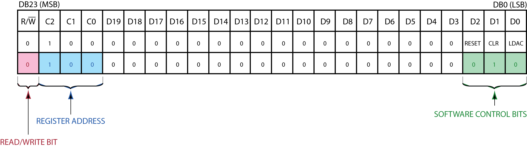
Figure 9. Clear the part to a user defined value
Readback the Clearcode Register
To confirm the clearcode value written to the part, read the data on the clearcode register (Full scale for this example). Write the following over the serial interface: 1011 XXXX XXXX XXXX XXXX XXXX.
Remember that this action is a read function, so the R/ bit is set to “1”.
The data bits are don't care, as the aim is to read from the part and not a write function.

Figure 10. Readback from the clearcode register
resources/quick-start/ad5791.1365516392.txt.gz · Last modified: 09 Apr 2013 16:06 by Estibaliz Sanz