This is an old revision of the document!
AD5696R/AD5695R/AD5694R Quick Start Guide
Quad, 16-/14-/12-Bit, Voltage Output, nanoDAC+™ with a 2 ppm/ºC Reference, I2C Interface
Features
High relative accuracy (INL): ±2
LSB maximum (16-bit
AD5696R)
Low drift 2.5
V on-chip reference: 2 ppm/°C typical temperature coefficient
Tiny 3 mm × 3 mm 16-lead LFCSP or 16-lead TSSOP package
Total unadjusted error (TUE): 0.1% of FSR maximum
Offset error: 1.5
mV maximum
Gain error: 0.1% of FSR maximum
High drive capability: 20
mA, 0.5
V from supply rails
User selectable gain of 1 or 2 (GAIN pin)
Reset to zero scale or midscale (RSTSEL pin)
1.8
V logic compatibility
-
2.7
V to 5.5
V power supply
−40°C to +105°C temperature range
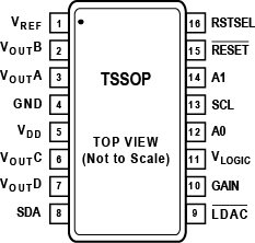
Pin Configurations: 16-Lead LFCSP (Left) and 16-Lead TSSOP (Right)
 <html> </html>

Table 1. Function Descriptions for Quick Start
| Mnemonic | Description |
| VOUTA | Analog output voltage from DAC A. |
| VOUTB | Analog output voltage from DAC B. |
| VOUTC | Analog output voltage from DAC A. |
| VOUTD | Analog output voltage from DAC D. |
| SDA | Connect to serial interface. |
| SCL | Connect to serial interface. |
| A1 | Address pin. |
| A0 | Address pin. |
| VREF | No connect. |
| VDD | Connect to 5 V supply. Decouple with 10 μF and 0.1 μF capacitors. |
| GND | Connect to ground. |
 | Tie low. |
| RSTSEL | Tie to GND to power up to zero scale. |
| GAIN | Tie to GND. DAC outputs have a span from 0 V to VREF. |
 | Tie high. |
| VLOGIC | Connect to serial interface supply voltage. |
Shift Register Contents
Table 2. Command Definitions
| Command | |
| C3 | C2 | C1 | C0 | Description |
| 0 | 0 | 0 | 0 | No operation |
| 0 | 0 | 0 | 1 | Write to Input Register n (dependent on LDAC) |
| 0 | 0 | 1 | 0 | Update DAC Register n with contents of Input Register n |
| 0 | 0 | 1 | 1 | Write to and update DAC Channel n |
| 0 | 1 | 0 | 0 | Power down/power up DAC |
| 0 | 1 | 0 | 1 | Hardware  mask register mask register |
| 0 | 1 | 1 | 0 | Software reset (power-on reset) |
| 0 | 1 | 1 | 1 | Internal reference setup register |
| 1 | 0 | 0 | 0 | Reserved |
| 1 | 0 | 0 | 1 | Reserved |
| 1 | 0 | 1 | 0 | Reserved |
| … | … | … | … | Reserved |
| 1 | 1 | 1 | 1 | Reserved |
Transfer Function
![V_OUT = V_REF * Gain delim{[}{D/2^N}{]} V_OUT = V_REF * Gain delim{[}{D/2^N}{]}](/lib/plugins/mathpublish/img.php?img=2193fe9f82af98c8c406656a81beb4cf)
where:
D is the decimal equivalent.
N is the number of bits.
Simple Write Example 1
To Update Channel A, write the following over the serial interface:
0001 XXX1 1000000000000000 (four command bits, four address bits, 16 data bits for the
AD5696R).
This updates Channel A to midscale. GAIN = 1,
VOUTA = 1.25
V.

Simple Write: Example 2
To update Channel B, write the following over the serial interface: 0001 XX1X 1000000000000000.
This updates Channel B to midscale. GAIN = 1,
VOUTB = 1.25
V.

Simple Write: Example 3
To update both Channel A and Channel B, write the following: 0001 XX11 1111111111111111.
This updates both channels to fullcale. GAIN = 1,
VOUTB = 2.5
V,
VOUTA = 2.5
V.

 This version (17 Apr 2012 20:17) is a draft.