
The AD7303 is a dual, 8-bit voltage out DAC that operates from a single 2.7V to 5.5V supply. Its on-chip precision output buffers allow the DAC outputs to swing rail-to-rail. This device uses a versatile 3-wire serial interface that operates at clock rates up to 30 MHz, and is compatible with QSPIm SPI, microwire and digital signal processor interface standards.
Two reference designs are available for this part:
The bit file provided in the project *.zip file combines the FPGA bit file and the SDK elf files. It may be used for a quick check on the system. All you need is the hardware and a PC running a UART terminal and the programmer (IMPACT).
If you are not familiar with LX9 and/or Xilix tools, please visit
products/boards-and-kits/AES-S6MB-LX9.htm for details.
If you are not familiar with Nexys™3 and/or Xilix tools, please visit
http://www.digilentinc.com/Products/Detail.cfm?NavPath=2,400,897&Prod=NEXYS3 for details.
If you are not familiar with ZedBoard and/or Xilix tools, please visit
http://www.em.avnet.com/en-us/design/drc/Pages/Zedboard.aspx for details.
Extract the project from the archive file (AD7303_<board_name>.zip) to the location you desire.
To begin, connect the PmodDA1 to J4 connector of LX9 board, pins 1 to 6 (see image below). You can use an extension cable for ease of use. Connect the USB cable from the PC to the USB-UART female connector of the board for the UART terminal. The board will be programmed through its USB male connector.
Extract the project from the archive file (AD7303_<board_name>.zip) to the location you desire.
To begin, connect the PmodDA1 to JA connector of Nexys™3 board, pins JA1 to JA6 (see image below). You can use an extension cable for ease of use. Connect the USB cables from the PC to the board, one for programming (Digilent USB device) and one for the UART terminal (FT232R USB UART).
To begin, connect the PmodDA1 to JD connector of ZedBoard (see image below). You can use an extension cable for ease of use. Connect the USB cables from the PC to the board, one for programming (Digilent USB device) and one for the UART terminal (FT232R USB UART).
Start IMPACT, and double click “Boundary Scan”. Right click and select Initialize Chain. The program should recognize the Spartan 6 device (see screenshot below). Connect an oscilloscope to the outputs of the PmodDA1 and then program the device using the bit file provided in the project *.zip archive, located in the “sw” folder (../ad7303/sw/AD7303.bit).
If programming was successful, the Main Menu will apear in your UART terminal, as seen in the picture below. There are 3 options:
When entering Fixed Value Mode, DAC selection is automatically activated. Selecting the DAC is done by pressing [1] to [4].
Fixed Value Mode allows entering a value between 0x00 and 0xFF, value that will be programmed in the DAC. If the number of input characters is less than 2 (e.g. f or 7), the [Enter] key must be pressed in order to validate the input. If 2 characters are input, the value is automatically validated (in order to prevent entering more than 2 characters). Pressing the [s] key at any time will enter DAC Selection Mode.
Pressing the [q] key at any time exits the Fixed Value (or Waveform Generation) Mode and displays the Main Menu again.
When entering Waveform Generation Mode, DAC selection is automatically activated. Selecting the DAC is done by pressing [1] to [4].
Waveform Generation Mode allows selecting between 4 types of waveforms: Square, Triangle, Sawtooth and Sine waveforms. Changing between the 4 is done by pressing [1] to [4] on the keyboard. Pressing [s] at any time will enter DAC Selection Mode. Pressing [q] at any time will return to the Main Menu.
Programmable Ramp Signal Generator allows generating a programmable ramp signal. This mode can be used to test the PmodDA1 using a Digital Multimeter.
Enter time step allows setting a time step between 100 and 5000 ms.
Enter increment size allows selecting an increment size that suits your design. Values can vary from 0x00 to 0xFF.
Select DAC allows selecting which DAC Output will be used for the Ramp Signal Generation.
Run Ramp Signal Generator will start generating the desired output.
Run the download.bat script from the “../bin” folder downloaded from the github (see the links in the download section of the wiki page). The script will automatically configure the ZYNQ SoC and download the *.elf file afterwards.
If the download script fails to run, modify the Xilinx Tools path in download.bat to match your Xilinx Installation path.
If programming was successful, you will be able to see a Triangle Waveform output on A1 and a Sine Waveform output on B1.
The reference design is a simple SPI interface with two MOSI pins for the PmodDA1. The software programs the device sending an 8-bit configuration value followed by 8-bit data value.
The hardware SPI access allows writing data to the AD7303, using a single CS and SCLK pins, and two MOSI pins (PmodDA1 contains two AD7303 Integrated Circuits, which share the same CS and SCLK pins, but have separate MOSI pins).
For the ZedBoard, DMA is used to send data from DDR to the AD7303 IP Core, outputting a triangle waveform and a sine waveform.
Avnet LX-9 MicroBoard:
Digilent Nexys™3:
Avnet ZedBoard:
====== Linux Device Driver ======
Connect PmodDA1 to the JB1 connector of the ZedBoard (upper row of pins).
===== Preparing the SD Card =====
In order to prepare the SD Card for booting Linux on the ZedBoard:
* Download the device tree: PmodDA1 Linux devicetree
* Follow the instructions on the following wiki page, but use the device tree downloaded on the previous step
* Linux with HDMI video output on the ZED and ZC702.
Make sure you have an HDMI monitor connected to the ZedBoard, plug in the SD Card and power on the board.
If everything is correct, the system should boot up. If you don't have an HDMI monitor, connect to the board via UART, Baud Rate 115200.
There are 2 ways to test the driver.
* Using the terminal window
* Using the ADI IIO Oscilloscope
===== Using the terminal window =====
Open a new terminal window by pressing Ctrl+Alt+T.
Navigate to the location of the device and identify it using the following commands:
<code>
cd /sys/bus/iio/devices/
ls
iio:device0 iio:device1 trigger0
cd iio\:device0
cat name
ad7303
</code>
If the cat name command doesn't return ad7303, then change the number of the iio:device, and check again.
<code>
cd ..
cd iio\:device1
cat name
</code>
To see the list of options that the AD7303 driver provides, type:
<code>
ls
buffer out_voltage0_powerdown out_voltage1_raw scan_elements uevent
dev out_voltage0_raw out_voltage_scale subsystem
name out_voltage1_powerdown power trigger
</code>
To set the raw output voltage, type:
<code>
echo 120 > out_voltage0_raw
</code>
To check that the raw output voltage has been set, you can type:
<code>
cat out_voltage0_raw
120
</code>
If you want to set the voltage for the second channel, replace out_voltage0_raw with out_voltage1_raw.
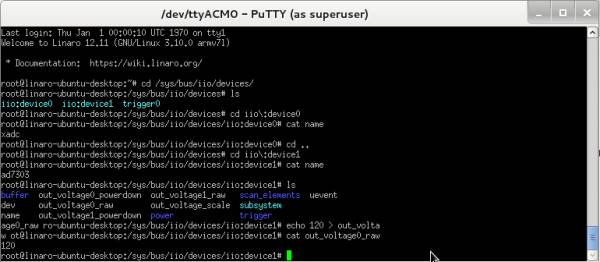
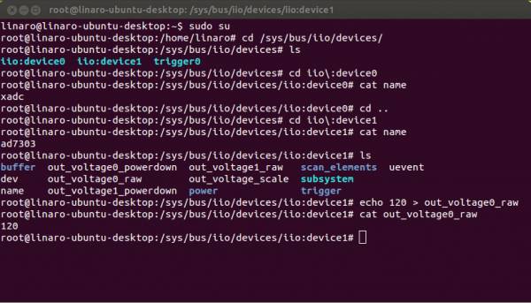 The commands written above can also be used if not using an HDMI monitor and a wireless keyboard, by using a serial terminal, and typing the commands after the system boot-up is complete.
 ===== Using the ADI IIO Oscilloscope =====
Install the ADI IIO Oscilloscope using the instructions from the following wiki page:
* IIO Oscilloscope
Launch the ADI IIO Oscilloscope.
Open the Settings menu and select Impulse generator submenu. A popup window will appear and allow you to select an impulse generator (a high resolution timer) and its frequency. The conversions for both the ADC and the DAC are started by the impulses of the generator. Click the OK button.
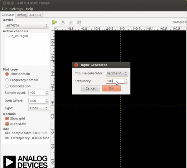 If the Impulse generator option is not available, you can configure the timer manually using the following commands:
<code>
cd /sys/bus/iio/devices
ls
iio:device0 iio:device1 trigger0
cd trigger0
echo 1000 > frequency
cat frequency
1000
</code>
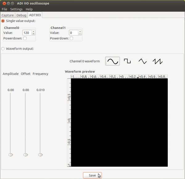
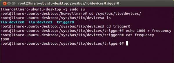 Select AD7303 tab from the top options. Click on Single value output, type in the desired value, and click Save at the bottom of the window.
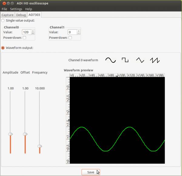
 Select AD7303 tab from the top options. Click on Waveform output, select the type of waveform, configure the desired Amplitude, Offset and Frequency, and click Save at the bottom of the window. PmodDA1 Channel0 should now be outputting the configured waveform.
 ====== AD7303 Pmod and AD7476 Pmod Reference Design ======
The bit file provided in the project *.zip file combines the FPGA bit file and the SDK elf files. It may be used for a quick check on the system.
If you are not familiar with Nexys3 and/or Xilix tools, please visit
http://digilentinc.com/Products/Detail.cfm?NavPath=2,400,897&Prod=NEXYS3 for details.
To begin, connect the PmodAD1 to JA1 connector of Nexys3 board, pins 1 to 6 (see image below) and the PmodDA1 to JB1 connector of Nexys3 board, pins 1 to 6. You can use an extension cable for ease of use. Connect the USB cables from the PC to the board.
Start IMPACT, and double click “Boundary Scan”. Right click and select Initialize Chain. The program should recognize the Spartan 6 device (see screenshot below). Program the FPGA using the download.bit file provided in the project *.zip archive, located in the “sw” folder (../ad7303_ad7476/sw/download.bit).
Start the ChipScope Pro Analyzer provided with the Xilinx ISE Design Suite 13.2 and load the project Nexys3_ChipScope_Demo.cpj located in the “chipscope” folder (../ad7303_ad7476/chipscope/Nexys3_ChipScope_Demo.cpj). Click the Open Cable/Search JTAG Chain button and afterwards double click Bus Plot and select Repetitive Trigger Run Mode. Click the Apply Settings and Arm Trigger button. On the main screen you will se the waveforms change once every 25 seconds, between Sine, Square, Sawtooth and Triangle waveforms. Each waveform has a period of 25ms. You can compare the waveform displayed in ChipScope Pro with the waveform displayed on an oscilloscope from the DAC output.