This document presents the steps to setup an environment for using the EVAL-CN0235-SDPZ evaluation board together with the Xilinx KC705 FPGA board and the Xilinx Embedded Development Kit (EDK). Below is presented a picture of the EVAL-CN0235-SDPZ Evaluation Board with the Xilinx KC705 board.
For component evaluation and performance purposes, as opposed to quick prototyping, the user is directed to use the part evaluation setup. This consists of:
The SDP-B controller board is part of Analog Devices System Demonstration Platform (SDP). It provides a high speed USB 2.0 connection from the PC to the component evaluation board. The PC runs the evaluation software. Each evaluation board, which is an SDP compatible daughter board, includes the necessary installation file required for performance testing.
Note: it is expected that the analog performance on the two platforms may differ.
Below is presented a picture of SDP-B Controller Board with the EVAL-CN0235-SDPZ Evaluation Board.
The CN0235 board is a fully isolated lithium ion battery monitoring and protection system. Lithium ion (Li-Ion) battery stacks contain a large number of individual cells that must be monitored correctly in order to enhance the battery efficiency, prolong the battery life, and ensure safety.
The AD7280A contains all the functions required for general-purpose monitoring of stacked lithium ion batteries as used in hybrid electric vehicles, battery backup applications, and power tools. The part has multiplexed cell voltage and auxiliary ADC measurement channels for up to six cells of battery management. An internal ±3 ppm/°C reference is provided that allows a cell voltage accuracy of ±1.6 mV. The ADC resolution is 12 bits and allows conversion of up to 48 cells within 7 us.
The AD8280 is a hardware-only safety monitor for lithium ion battery stacks. The part has inputs to monitor six battery cells and two temperature sensors (either NTC or PTC thermistors). The part is designed to be daisy-chained with other AD8280 devices to monitor a stack of significantly more than six cells without the need for numerous isolators. Its output can be configured for an independent or shared alarm state.
The first objective is to ensure that you have all of the items needed and to install the software tools so that you are ready to create and run the evaluation project.
Before connecting the ADI evaluation board to the Xilinx KC705 make sure that the VADJ_FPGA voltage of the KC705 is set to 3.3V. For more details on how to change the setting for VADJ_FPGA visit the Xilinx KC705 product page.
The following commands were implemented in this version of EVAL-CN0235 reference project for Xilinx KC705 FPGA board.
| Command | Description |
|---|---|
| help? | Displays all available commands. |
| adcCode? | Displays the ADC code of one channel from selected device. Accepted values: device: 0 - master 1 - slave register address: 0 - Cell Voltage 1 1 - Cell Voltage 2 2 - Cell Voltage 3 3 - Cell Voltage 4 4 - Cell Voltage 5 5 - Cell Voltage 6 6 - AUX ADC 1 7 - AUX ADC 2 8 - AUX ADC 3 9 - AUX ADC 4 10 - AUX ADC 5 11 - AUX ADC 6 |
| voltage? | Displays the input voltage of one channel from selected device. Accepted values: device: 0 - master 1 - slave register address: 0 - Cell Voltage 1 1 - Cell Voltage 2 2 - Cell Voltage 3 3 - Cell Voltage 4 4 - Cell Voltage 5 5 - Cell Voltage 6 6 - AUX ADC 1 7 - AUX ADC 2 8 - AUX ADC 3 9 - AUX ADC 4 10 - AUX ADC 5 11 - AUX ADC 6 |
| register? | Displays the content of one register from selected device. Accepted values: device: 0 - master 1 - slave register address: 13 - Control high byte 14 - Control low byte 15 - Cell Overvoltage 16 - Cell Undervoltage … (see AD7280A_Datasheet p.28) 29 - CNVST Control |
| register= | Sets the content of one register from selected device. Accepted values: device: 0 - master 1 - slave register address: 13 - Control high byte 14 - Control low byte 15 - Cell Overvoltage 16 - Cell Undervoltage … (see AD7280A_Datasheet p.28) 29 - CNVST Control register value: 0 .. 255 - value to be written inside the register. |
| selfTestAD7280A! | Performs the self test for both AD7280A devices on the board (one master and one slave). |
| alertPinAD7280A? | Reads the status of Alert Pin from AD7280A. |
| enableAD8280= | Enables/disables the AD8280 device. Accepted values: 0 - disable the AD8280 device 1 - enable the AD8280 device |
| alarmPinOvAD8280? | Reads the status of Overvoltage Alarm Pin from AD8280. |
| alarmPinUvAD8280? | Reads the status of Undervoltage Alarm Pin from AD8280. |
| selfTestAD8280! | Performs the self test for both AD8280 devices on the board (one master and one slave). |
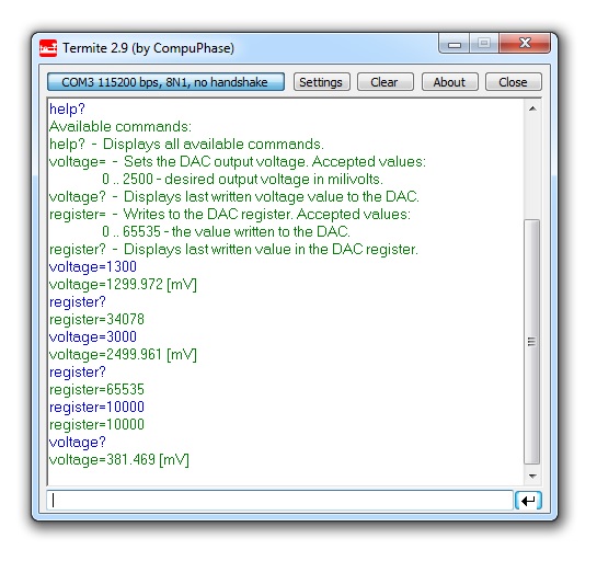
Commands can be executed using a serial terminal connected to the UART peripheral of Xilinx KC705 FPGA.
The following image shows a generic list of commands in a serial terminal connected to Xilinx KC705 FPGA's UART peripheral.

The hardware platform for each reference projects with FMC-SDP interposer and KC705 evaluation board is common. The next steps should be followed to recreate the software project of the reference design: