 This version (31 Oct 2013 10:59) was approved by Istvan Csomortani.The Previously approved version (19 Nov 2012 18:57) is available.
This is an old revision of the document!
This document presents the steps to setup an environment for using the EVAL-ADF4106SD1Z evaluation board together with the Xilinx KC705 FPGA board and the Xilinx Embedded Development Kit (EDK). Below is presented a picture of the EVAL-ADF4106SD1Z Evaluation Board with the Xilinx KC705 board.
For component evaluation and performance purposes, as opposed to quick prototyping, the user is directed to Analog Devices System Demonstration Platform (SDP). The SDP consists of a:
The EVAL-SDP-CS1Z controller board is Serial Interfaces Only, low cost, reduced functionality controller board. It has a USB to Serial Engine at its core. It connects to the PC through a USB 2.0 high speed port. The SDP-S has a single 120 pin connector and exposes SPI, I2C and GPIO interfaces to connected SDP daughter boards.
The EVAL-ADF4106SD1Z is designed to allow the user to evaluate the performance of the ADF4106 frequency synthesizer for phase-locked loops (PLLs). Figure 1 shows the board, which contains the ADF4106 synthesizer, an SMA connector for the reference input, power supplies, and an RF output. There is also a footprint for a loop filter and a VCO on board.
The ADF4106 frequency synthesizer can be used to implement local oscillators in the up-conversion and down-conversion sections of wireless receivers and transmitters. It consists of a low noise, digital phase frequency detector (PFD), a precision charge pump, a programmable reference divider, programmable A counter and B counter, and a dual-modulus prescaler (P/P + 1). The A (6-bit) counter and B (13-bit) counter, in conjunction with the dual-modulus prescaler (P/P + 1), implement an N divider (N = BP + A). In addition, the 14-bit reference counter (R Counter) allows selectable REFIN frequencies at the PFD input. A complete phase-locked loop (PLL) can be implemented if the synthesizer is used with an external loop filter and voltage controlled oscillator (VCO). Its very high bandwidth means that frequency doublers can be eliminated in many high frequency systems, simplifying system architecture and reducing cost.
The first objective is to ensure that you have all of the items needed and to install the software tools so that you are ready to create and run the evaluation project.
Before connecting the ADI evaluation board to the Xilinx KC705 make sure that the VADJ_FPGA voltage of the KC705 is set to 3.3V. For more details on how to change the setting for VADJ_FPGA visit the Xilinx KC705 product page.
The following commands were implemented in this version of EVAL-ADF4106SD1Z reference project for Xilinx KC705 FPGA board.
| Command | Description |
|---|---|
| help? | Displays all available commands. |
| setregister= | Update the selected latch with the current set ups. Accepted value: latch: 0 - Reference latch 1 - N Counter Latch 2 - Function Latch 3 - Initialization Latch value: 24 bit values, you can find more information about the registers in the data sheet |
| getregister? | Print the specified latch values in a human readable format. Accepted value: latch: 0 - Reference latch 1 - N Counter Latch 2 - Function Latch 3 - Initialization Latch |
| setfrequency= | Set the VCO frequency. Accepted value: 5 .. 6000 - betwwen 5Mhz and 6Ghz |
| getfrequency? | Print the actual VCO frequency. |
Commands can be executed using a serial terminal connected to the UART peripheral of Xilinx KC705 FPGA.
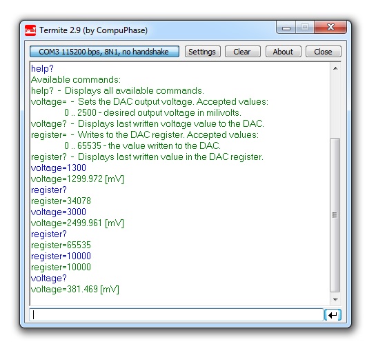
The following image shows a generic list of commands in a serial terminal connected to Xilinx KC705 FPGA's UART peripheral.

The hardware platform for each reference projects with FMC-SDP interposer and KC705 evaluation board is common. The next steps should be followed to recreate the software project of the reference design: