This document presents the steps to setup an environment for using the EVAL-AD5757SDZ evaluation board together with the Xilinx KC705 FPGA board and the Xilinx Embedded Development Kit (EDK). Below is presented a picture of the EVAL-AD5757SDZ Evaluation Board with the Xilinx KC705 board.
For component evaluation and performance purposes, as opposed to quick prototyping, the user is directed to use the part evaluation setup. This consists of:
The SDP-B controller board is part of Analog Devices System Demonstration Platform (SDP). It provides a high speed USB 2.0 connection from the PC to the component evaluation board. The PC runs the evaluation software. Each evaluation board, which is an SDP compatible daughter board, includes the necessary installation file required for performance testing.
Note: it is expected that the analog performance on the two platforms may differ.
Below is presented a picture of SDP-B Controller Board with the EVAL-AD5757SDZ Evaluation Board.
The AD5757 is a quad, current output DAC that operates with a power supply range from 10.8 V to 33 V. On-chip dynamic power control minimizes package power dissipation by regulating the voltage on the output driver from 7.4 V to 29.5 V using a dc-to-dc boost converter optimized for minimum on-chip power dissipation. Each channel has a corresponding CHART pin so that HART signals can be coupled onto the current output of the AD5757.
The EVAL-AD5757SDZ evaluation board is designed to help customers quickly prototype new AD5757 circuits and reduce design time. To power the AD5757SDZ evaluation board supply 15V between the AVSS (0V) and AVDD (+15V) inputs for the analog supply and 5V between PGND(0V) and AVCC(+5V) as DC-to-DC supply voltage.
The first objective is to ensure that you have all of the items needed and to install the software tools so that you are ready to create and run the evaluation project.
Before connecting the ADI evaluation board to the Xilinx KC705 make sure that the VADJ_FPGA voltage of the KC705 is set to 3.3V. For more details on how to change the setting for VADJ_FPGA visit the Xilinx KC705 product page.
To power on the EVAL-AD5757 evaluation board, you need to provide an external +15V AVdd and -15V AVss analog supply voltage and a +5V AVcc DC-to-DC supply voltage, which will supplies all four on-board dc-to-dc blocks and may draw as much as 0.8 A peak current per channel (for more information see: EVAL-AD5757SDZ evaluation board user guide).
The following commands were implemented in this version of EVAL-AD5757 reference project for Xilinx KC705 FPGA board.
| Command | Description |
|---|---|
| help? | Displays all available commands. |
| register= | Writes to the a data register. Accepted values: Register address: 0 - DAC Data Reg 2 - Gain Register 3 - Gain Register All DACs 4 - Offset Register 5 - Offset Register All DACs 6 - Clear Code Register 7 - Control Register Channel: 0 .. 3 - channel A .. D. Value: 0 .. 65535 - the value written to the DAC. |
| control= | Writes to the a control register. Accepted values: Register address: 0 - Slew Rate Register 1 - Main Control Register 2 - DAC Control Register 3 - Dc-to-dc Control Register 4 - Software Register Channel: 0 .. 3 - channel A .. D. Value: 0 .. 65535 - the value written to the DAC. |
| register? | Read back the value of a specified register. Accepted values: Register address : 0x00 .. 0x1A. |
| power= | Set the power state of the dc-to-dc converters, DAC and internal amplifiers for the selected channel. Accepted values: Channel: 0 .. 3 - channel A .. D. Value: 0 - turn off; 1 - turn on. |
| power? | Displays the power state of the dc-to-dc converters,DAC and internal amplifiers for the selected channel. Accepted values: Channel: 0 .. 3 - channel A .. D. |
| range= | Set the range of the selected channel. Accepted values: Channel: 0 .. 3 - channel A .. D. Range: 0 - 0 V to 5 V voltage 1 - 0 V to 10 V voltage 2 - -5 V to +5 V voltage 3 - -10 V to +10 V voltage 4 - 4 mA to 20 mA current 5 - 0 mA to 20 mA current 6 - 0 mA to 24 mA current |
| range? | Displays the range of the selected channel. Accepted values: Channel: 0 .. 3 - channel A .. D. |
| voltage= | Sets the output voltage for a selected channel. Accepted values: Channel: 0 .. 3 - channel A .. D. Desired voltage(unit in V) multiplied by 1000 |
| voltage? | Displays the output voltage for a selected channel. Accepted values: Channel: 0 .. 3 - channel A .. D. |
| current= | Displays the output current for a selected channel. Accepted values: Channel: 0 .. 3 - channel A .. D. Desired current (unit in mA) multiplied by 1000 |
| current? | Displays the output current for a selected channel. Accepted values: Channel: 0 .. 3 - channel A .. D. |
| getStatus! | Read back the Status register and print any faults or errors. |
| testSPI! | Ensure that the SPI interface are working correctly. |
Commands can be executed using a serial terminal connected to the UART peripheral of Xilinx KC705 FPGA.
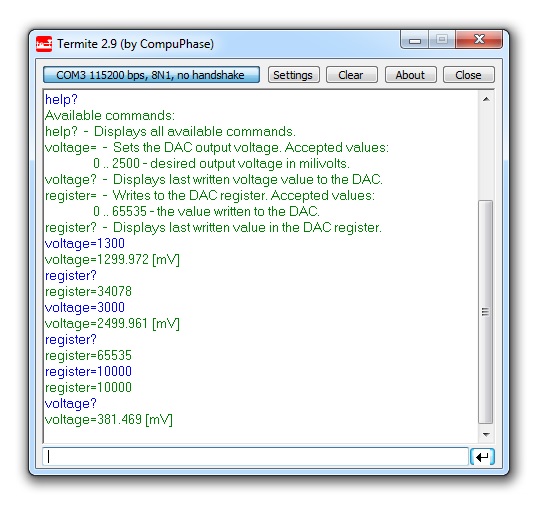
The following image shows a generic list of commands in a serial terminal connected to Xilinx KC705 FPGA's UART peripheral.

The hardware platform for each reference projects with FMC-SDP interposer and KC705 evaluation board is common. The next steps should be followed to recreate the software project of the reference design: