


This version (18 May 2022 14:33) was approved by Erlandas Petkevicius.
Using the Serial Peripheral Interface on the AD5758
The AD5758/ADFS5758/AD5753/AD5423/AD5413 contain the same serial peripheral interface and follow the below guide.
The AD5758 is controlled over a 4-wire serial interface with an 8-bit cyclic redundancy check (CRC-8) enabled by default. The input shift register is 32 bits wide, and data is loaded into the device MSB first under the control of a serial clock input, SCLK. Data is clocked in on the falling edge of SCLK. If CRC is disabled, the serial interface is reduced to 24 bits; a 32-bit frame is still accepted but the last 8 bits are ignored. The purpose of this guide is to explain how the AD5758 SPI works and show examples of the first required SPI writes including CRC as recommended in Figure 90 of the AD5758 datasheet.
SPI Modes
SPI has 4 modes that it operates in. The CPOL bit sets the clocks polarity during the idle state. The CPHA bit selects the clock phase. For mode 0 and mode 1, the idle clock state is low. For mode 2 and mode 3, the idle clock state is high. The CPOL and CPHA bits decide on which edge the data is sampled and shifted. The Mode Table below demonstrates SPI modes. The AD5758 (and all other generics listed in the INFO) can be used in either mode 1 or mode 2.
SPI Mode Table
| SPI Mode | CPOL | CPHA | Clock Polarity in Idle State | Clock phase used to Sample Edge |
|---|---|---|---|---|
| 0 | 0 | 0 | Logic Low | Data shifted out on falling edge and sampled on the rising edge |
| 1 | 0 | 1 | Logic Low | Data shifted out on the rising edge and sampled on the falling edge |
| 2 | 1 | 0 | Logic High | Data shifted out on the rising edge and sampled on the falling edge |
| 3 | 1 | 1 | Logic High | Data shifted out on the falling edge and sampled on the rising edge |
SPI Cyclic Redundancy Check (CRC)
To verify that data has been received correctly in noisy environments, the AD5758 offers the option of CRC based on a CRC-8. The device controlling the AD5758 generates an 8-bit frame check sequence using the following polynomial:
This sequence is added to the end of the 24 bit data-word, and 32 bits are sent to the AD5758 before taking SYNC high.
If the CRC check is valid, the data is written to the selected register. If the CRC check fails, the data is ignored and the SPI_CRC_ERR bit is set along with the fault pin being asserted. The SPI CRC feature can be used for both the transmission and receipt of data packets. The CRC is enabled by default so the user must supply a frame of exactly 32 bits wide that contains the 24 data bits and 8-bit CRC for the first SPI write. To disable the CRC (Bit 0 SPI_CRC_EN in register 0x10) it is recommended to do this after the calibration memory refresh step.
Writing to a Register
As shown in the SPI Write Frame table, every SPI write frame contains a slip bit, two address bits, a register address, data and if enabled the CRC will be appended to the SPI frame creating a 32 bit frame. The slip bit must equal the inverse of the MSB − 1 for the frame to be considered valid. The address bits must match the hardware address pins (AD0 and AD1) for the device to accept the SPI frame on the bus. The register address is the address of the register the data will be written to.
SPI Write Frame
| D31 | D30:D29 | D28:D24 | D23:D8 | D7:D0 |
|---|---|---|---|---|
| Slip Bit | Address Bits | Register Address | Data | CRC |
With CRC enabled (default state), the input shift register is 32 bits wide. Data is loaded into the device MSB first, under the control of a serial clock input, SCLK. Data is clocked in on the falling edge of SCLK. If CRC is disabled, the serial interface is reduced to 24 bits; a 32-bit frame is still accepted but the last 8 bits are ignored.
Reading a Register
The default mode for reading back a register is called the two stage readback mode. This mode consists of a write to the TWO_ STAGE_READBACK_SELECT register (Address 0x13) to select the register location to be read back, followed by a NOP command. To perform a NOP command, write all zeros to Bits[D15:D0] of the NOP register (Address 0x00). See the product datasheet for other readback modes.
SPI Read Frame
| D31:30 | D29 | D28:D24 | D23:D8 | D7:D0 |
|---|---|---|---|---|
| 10 | Fault Pin Status | Register Address | Data | CRC |
Performing a Software Reset
Before initially configuring the device, it is good practice to perform either a hardware or software reset. A software reset is performed by writing 2 keys (0x15FA and 0xAF51) respectively to the key (address 0x08) register. The hardware address pins (AD0 and AD1) are assumed to be logic low for all the following SPI transactions.
Figures 1 and 2 show the first and second software reset key writes. The first write of 0x8815FAA4 can be decoded as
| D31 | D30:D29 | D28:D24 | D23:D8 | D7:D0 |
|---|---|---|---|---|
| Slip Bit | Address Bits | Register Address | Data | CRC |
| 1 | 00 | 0x08 (01000) | 0x15FA | 0xA4 |
For the second write the data has changed to 0xFA51 and the CRC changed to 0x31.
The oscilloscope plots below show each of the 4 SPI wire data:
SCLK --> SPI clock
SYNC --> SYNC signal (must be taken low to initiate SPI transfer)
SDI --> Serial Data In (Top line of S1 serial bus)
SDO --> Serial Data Out (Bottom line of S1 serial bus)
In the following examples the software driver is configured for SPI mode 1 and the CRC is enabled.
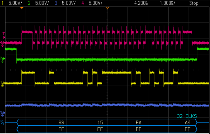
Figure 1 Software Reset Key1 Write 0x8815FAA4

Figure 2 Software Reset Key2 Write 0x88AF5131
Figure 3 shows a readback of the default state of the digital diagnostic results register (Address 0x14) before the calibration memory has been refreshed. There are 2 SPI frames visible in the scope plot. Figures 4 and 5 show the first and second SPI frames respectively. The first being the readback command to read the digital diagnostic results register (Address 0x14) and the second shows the NOP command along with the readback data on SDO. The readback data 0x94A0001A on SDO can be decoded as Bits 31:30 = 10, Fault pin status = 0. Register Address = 0x14, Data = 0xA000 (CAL_MEM_UNREFRESHED = 1 and RESET_OCCURED = 1), CRC = 0x1A

Figure 3 Two Stage Readback command

Figure 4 Two Stage Readback command - first frame write 0x93001478

Figure 5 Two Stage Readback command - second frame write 0x8000000B (including SDO data 0x94A0001A)
Calibration Memory Refresh
After performing a software or hardware reset the next write must be a calibration memory refresh. The refresh is performed by writing the key 0xFCBA to the key register (address 0x08). The calibration memory refresh SPI write is 0x88FCBA9D.
Disabling CRC
After performing a calibration refresh the CRC can be disabled if desired. The command to disable the CRC is Figure 4 shows the SPI write to clear the reset occurred bit. The SPI write to disable the CRC is 0x50005CB7.
Clearing Reset Occurred
After performing a calibration refresh the device can now be configured as required. The reset occurred bit (Bit 13) in the digital diagnostic results register (Address 0x14) is a logic high and should be cleared. To clear the bit a “1” must be written to clear the bit to a logic 0. The SPI write to clear the reset occurred bit is 0x942000AC.
resources/eval/user-guides/spi.txt · Last modified: 18 May 2022 13:59 by valerie hamilton