


No renderer 'pdf' found for mode 'pdf'
This version (16 Jun 2023 10:07) was approved by John Marco Mina.The Previously approved version (16 Jun 2023 09:56) is available.
Table of Contents
EVALUATING THE AD9148 DIGITAL-TO-ANALOG CONVERTER
Preface
This user guide describes both the hardware and software setup needed to acquire data capture from AD9148-EBZ & AD9148-M5375-EBZ evaluation board to characterize AD9148 Quad 16-bit 1GSPS TxDAC+® digital-to-analog converter.
This guide shows how AD9148-EBZ & AD9148-M5375-EBZ works with SDP-H1 / ADS7-V2 controller boards developed by Analog Devices. Link to the previous user guide document is provided for customers who still have the DPG3 controller board.
Tip: Click on any picture in this guide to open an enlarged version.
Typical Setup
 Figure 1a. AD9148-EBZ Setup with SDP-H1
 Figure 1b. AD9148-M5375-EBZ Setup with SDP-H1
 Figure 1c. AD9148-EBZ Setup with ADS7-V2
 Figure 1d. AD9148-M5375-EBZ Setup with ADS7-V2
Helpful Files:
- User Guide for DPG3 users:UG-1631
- Datasheet AD9148
- IBIS Model AD9148
- Schematics AD9148-EBZ-RevB | AD9148-M5375-EBZ-RevB
- Bill of Materials AD9148-EBZ-RevB | AD9148-M5375-EBZ-RevB
- PCB Gerber Files AD9148-EBZ-RevB | AD9148-M5375-EBZ-RevB
- PCB Board Files AD9148-EBZ-RevB | AD9148-M5375-EBZ-RevB
- PCB Layout AD9148-EBZ-RevB | AD9148-M5375-EBZ-RevB
Software Needed:
- DPG Lite (installed with ACE)
Do not install ACE on a computer with DAC Software Suite.
Hardware Needed:
- AD9148-EBZ / AD9148-M5375-EBZ Evaluation Board
- AD-DAC-FMC-ADP High-Speed DAC Evaluation Board to FMC Adaptor Board
- PC with ACE and DPG Lite Software Applications
- 5Vdc Power Supply
- (2) Banana Plug Cables
- High-Frequency Continuous Wave Generator
- Signal/Spectrum Analyzer
- USB-A to USB-Mini Cable
- (2) SMA Cables
- The following are included in SDP-H1 Evaluation Kit:
- 12Vdc Wall Adapter
- USB-A to USB-Mini Cable
- The following are included in ADS7-V2 Evaluation Kit:
- 12Vdc Power Supply
- Power Cord
- USB-A to USB-B Cable
Quick Start Guide
- Follow the Evaluation setup in Figure 1a, 1b, 1c, and 1d.
- Attach the evaluation board to SDP-H1 / ADS7-V2 FMC connector using the AD-DAC-FMC-ADP adapter board.
- Connect the continuous wave generator for clock input to J1.
- Connect the DAC output from J3 to a signal/spectrum analyzer.
- Connect the evaluation board to PC via USB and to a 5V 1A power supply via banana plug cables. If using the AD9148-M5375-EBZ evaluation board, increase the supply current limit to 1.5A.
- Connect SDP-H1/ADS7-V2 to PC via USB and to a 12Vdc power supply.
- Set clock input to 400MHz and 3dBm.
- Open ACE. The board will automatically be recognized by the software. Otherwise, install the plugin for AD9148-EBZ / AD9148-M5375-EBZ evaluation board. Then modify the configuration as shown in Figure 2a and Figure 2b, and click “Apply”.
 Figure 2a. ACE Initial Configuration Wizard on AD9148-EBZ Evaluation board
 Figure 2b. ACE Initial Configuration Wizard on AD9148-M5375-EBZ Evaluation board
- Open DPGDownloaderLite. The evaluation board, controller board and DCO Frequency of 100MHz will be automatically recognized by DPG.
- From DPGDownloaderLite, Add Generator Waveforms pulldown menu select Single Tone and apply the settings as shown in Figure 3. Set the Data Rate to 100MHz and Desired frequency to 15MHz. Set DAC resolution to the DAC’s number of bits to 16. Check the “Generate Complex Data (I & Q)” box then uncheck the “Unsigned Data” box.
- Select the in-phase tone from the I Data Vector pulldown menu and the quadrature tone from the Q Data Vector pulldown menu.
 Figure 3. DPGDownloaderLite Waveform Configuration for AD9148-EBZ / AD9148-M5375-EBZ
- Press the download arrow and then the play button. The spectrum similar to Figure 4 should appear in the signal/spectrum analyzer.
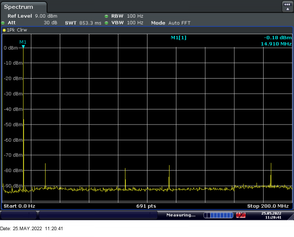 Figure 4. AD9148-EBZ FFT for Fdac=400MHz,4x Interpolation Fout=15MHz


Reconfiguring the Evaluation Board
This section details the quick start procedures for setting up the AD9148-EBZ & AD9148-M5375-EBZ evaluation board. Refer to the sections below to configure the power supply and the Reference & synchronization clock, as well as the Hardware provisions for the power supply.
Power Supply Configuration
The evaluation board has a provision for On-board or external power supply configuration.
Internal Power Supply
On-board power supply is implemented by default. JP1 selects the supply voltage level for IOVDD. Refer to Figure 5.
- When Pin 1 and Pin 2 are connected, IOVDD = 3.3 V (Default)
- When Pin 2 and Pin 3 are connected, IOVDD = 1.8 V


Figure 5. AD9148-EBZ JP1/AD9148-M5375-EBZ JP1


External Power Supply
To implement external supply configuration, remove the header shunt of six pin jumpers, as shown in Figure 6. Refer to Table 1 for external supply jumper connection.


Figure 6. AD9148-EBZ/AD9148-M5375-EBZ Pin Jumpers
 Table 1. AD9148-EBZ/AD9148-M5375-EBZ Jumper Connection
Other Provisions
The AD9148-EBZ and AD9148-M5375-EBZ have test points (TP) to check the power supplies on the board. Measure the supply rail (Red TP) and use the nearest grounding (black TP) as reference. See Table 2 and Table 3 below.
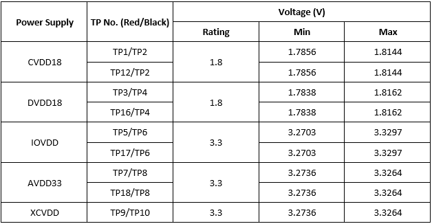 Table 2. AD9148-EBZ TP measurements
 Table 3. AD9148-M5375-EBZ TP measurements
Reference and Synchronization Clock
JP15 and JP18 selects the source for the reference and synchronization clock of the AD9148. the on-board clocking is implemented by default. Refer to Figure 7 to reconfigure the reference/ synchronization clock.
- On-board (from AD9516), center pads connected to inner pad.
- Off board (External source), center pads connected to outer pad.
 Figure 7. AD9148-EBZ/AD9148-M5375-EBZ Clock Source Configuration

Troubleshooting
This section lists items to check and practices to use when debugging any unexpected performance of a board. If unexpected results occurs:
- Restart the program by stopping pattern generation and issuing a power cycle. Power down the whole system by disconnecting the clock source / continuous wave generator and the supply for the controller (SDP-H1/ADS7-V2EBZ), then power up the system again following the steps in the Quick Start Guide.
- Double check the supply levels indicated in Table 2 and Table 3 in the “Other Provisions” section in Power Supply Configuration Section. If the voltages are not within the specified ratings, check if there are problems on component assembly or look for damaged ICs. Re-solder or replace components if necessary.
- If signal amplitude is lower than expected, compare spectrum analyzer settings to the recommended setup in the Quick Start Guide. Check for loose cable connections or try changing SMA-to-BNC cables. Loose connections and cable damage cause impedance mismatch.
- If there is no output at all, check if the power supply voltage drops to lower than 5V. If so, increase the supply current limit to greater than 1A until the voltage stabilizes to 5V.
- If there is still no output, check if clock input to AD9148 is stable by measuring clock leakage. Connect one of the evaluation board outputs to a spectrum analyzer. Boards and the clock source should be powered up but the DAC should not be generating a pattern. A low-power tone should be detected at the clock frequency. Otherwise, the clock source is not properly driving the clock input pins. Try increasing clock source / wave generator output signal level slowly up to 10 dBm.
resources/eval/dpg/eval-ad9148.txt · Last modified: 16 Jun 2023 10:07 by John Marco Mina