AD9106 & AD9102 Evaluation Boards
Preface
This page contains resources and documentation for evaluating the AD9106/AD9102 180 Msps 12-/14-bit quad/single DAC and waveform generator.
The AD9106-ARDZ-EBZ and AD9102-ARDZ-EBZ evaluation boards share the same PCB design, are compatible with ARM-based Mbed-enabled boards like SDP-K1 and are designed to connect to Arduino Uno headers. Both boards can be operated using either the Example Mbed Program or the Analysis Control Evaluation (ACE) Software. Links to the user guides are provided.
The AD910x-ARDZ-EBZ evaluation setup can be powered by USB only and does not require a high-frequency waveform generator for clock input. The evaluation board has an on-board 156.25 MHz crystal oscillator. To fit the evaluation system in a small form factor and manage power consumption within USB specifications, AD9106 and AD9102 supply voltages AVDD, DVDD and CLKVDD are limited to 3.3V only.
Included also in this page are resources and documentation for the obsolete AD9106-EBZ and AD9102-EBZ boards. These are standalone boards with the same PCB design and are controlled using a Labview-based GUI.
Typical Setup
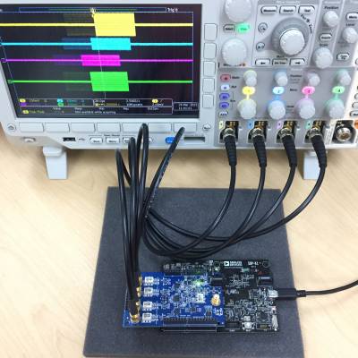 Figure 1a. AD9106-ARDZ-EBZ Typical Evaluation Setup
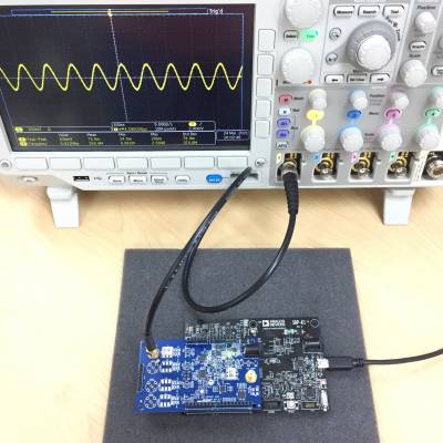 Figure 1b. AD9102-ARDZ-EBZ Typical Evaluation Setup
Tip: Click on any picture in this guide to open an enlarged version.
Helpful Files & Links
Hardware Needed
Minimum:
Additional:
Quick Start Guide
Reconfiguring the Evaluation Board
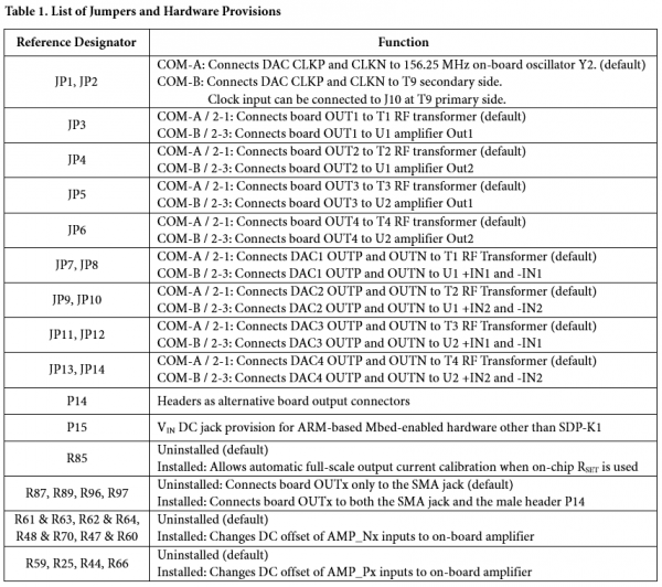
On-board jumpers and other hardware provisions are listed, and their functions described in Table 1. Meanwhile, the test points are enumerated and described in Table 2.

Clock Configuration
The evaluation board has a provision for on-board or external clocking configuration.
The on-board clocking configuration is implemented by default. DAC CLKP and CLKN are connected to the differential outputs of the on-board crystal oscillator as shown in Figure 2a. The onboard oscillator has a frequency of 156.25
MHz. If a different clock frequency is desired, Use external clocking configuration.
For external clocking configuration, change JP1 and JP2 connections first as shown in Figure 2b. Connect a High-frequency Continuous Wave Generator set to the desired frequency with 0dBm level to J10. The user will be prompted to enter the DAC Clock Input frequency in the ACE Board configuration wizard.

Figure 2a. DAC clock is connected to on-board oscillator (default) | Figure 2b. DAC clock is connected to J10
Output Configuration
The evaluation board has a provision to connect the DAC Outputs to the RF Balun Transformer or an 0n-board ADA4817-2 Amplifiers.
When tapping to the evaluation board outputs, users are not limited to the SMA jacks. P14 headers are provided as alternative connectors but performance is not as good as when using SMA connectors.
The DAC outputs are connected to the RF Balun Transformer by default as shown in figure 3.
To use On-board ADA4817-2 Amplifiers, change JP1 and JP2 connections as shown in Figure 4. Ensure that a 7V to 12V 30W Wall Wart is connected to P15. The user should also select the On-Board amplifier DAC Output setting in the ACE Board Configuration wizard.

Figure 3a. SMA output connectors are connected to RF transformers (default)

Figure 3b. SMA output connectors are connected to ADA4817-2 amplifier outputs

Figure 4a. DAC outputs are connected to RF transformers (default) | Figure 4b. DAC ouputs are connected to ADA4817-2 amplifiers
To properly observe the other patterns out of the amplifiers, replace C25, C26, C54, and C55 with 0Ω resistors or remove the capacitors then solder each pair of pads together. Waveforms are shown in Figures 17a to 18c.
The common-mode voltage of the amplifier outputs can also be changed by installing resistors for DC offset correction of amplifier inputs. Refer to Table 1. Keep C25, C26, C54, and C55 pads shorted.

The on-board amplifiers can be characterized using off-board power supplies by removing E1 and E2 then connecting 5.2V 0.2A across TP5 and ground and -5.2V 0.2A across TP4 and ground. Refer to Table 2.
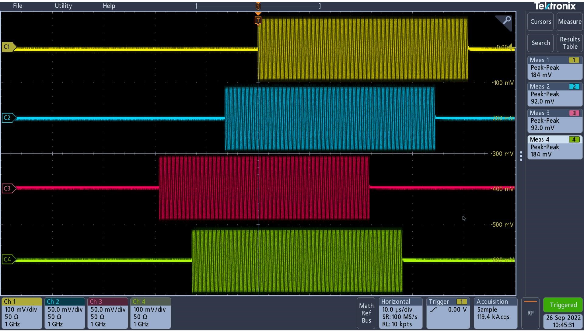 |  |
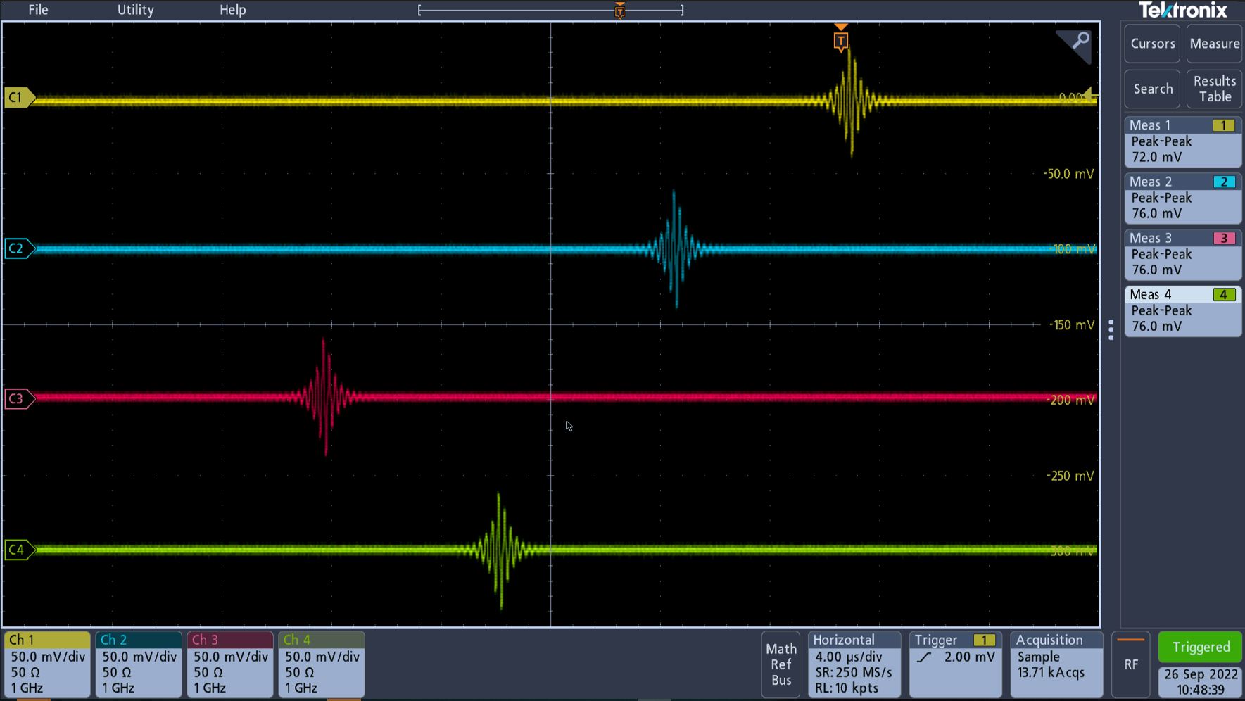
| Figure 5a. AD9106 4 Pulsed DDS-Generated Sine Wave from a Pre stored waveform with Different Start Delay and Digital Gain Settings | Figure 5b. AD9102 Pulsed DDS-Generated Sine Wave from a Pre stored waveform |
 | 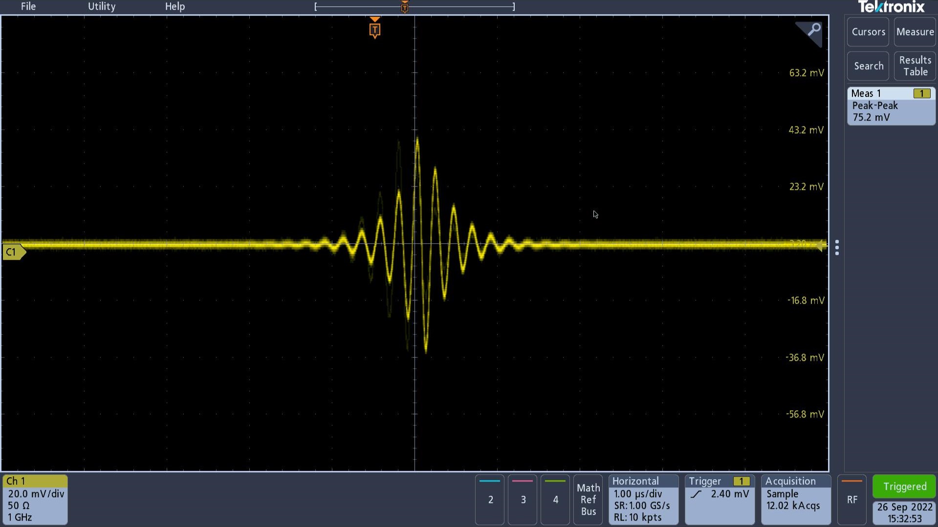 |
| Figure 6a. AD9106 Pulsed DDS-Generated Sine Wave modulated by an SRAM Vector with Different Start Delay | Figure 6b. AD9102 Pulsed DDS-Generated Sine Wave modulated by an SRAM Vector |
Troubleshooting
This section lists items to check and practices to use when debugging any unexpected performance of a board. If unexpected results occur
Restart the program by stopping pattern generation and pressing “Disconnect” from the terminal window. Press “Connect” again then follow the application menu.
Power down the whole system by disconnecting the wall wart, if using, and the
USB cable from SDP-K1, then power up the system again following the steps in the Quick Start Guide.
Measure voltages on the evaluation board. Refer to Table 2. If the voltages are off by 10% or more from the rated values, check if there are problems on component assembly or look for damaged ICs. Re-solder or replace components if necessary.
If signal amplitude is lower than expected, compare oscilloscope settings to the recommended setup in the Quick Start Guide. Check for loose cable connections or try changing SMA-to-BNC cables. Loose connections and cable damage cause impedance mismatch.
If there is no output at all, check if clock input to AD9106 / AD9102 is stable by measuring clock leakage. Connect one of the evaluation board outputs to a spectrum analyzer. Boards and the clock source should be powered up but the DAC should not be generating a pattern. A low-power tone should be detected at the clock frequency. Otherwise, the clock source is not properly driving the clock input pins. Try using an off-board continuous waveform generator as clock source or if already using, try increasing waveform generator output signal level to 3
dBm.
AD910x-EBZ (Obsolete) Documentation

