


This version (04 Jun 2021 04:52) was approved by Mar Christian Lacida.
Table of Contents
Evaluation Board for the ADG5401F Digital-To-Analog Converter Output Protection
Features
Evaluation Kit Contents
- EVAL-ADG5401FSDZ Evaluation Board
Equipment Needed
- PC running Windows®
- USB 2.0 port and USB 2.0 High-speed A to B Cable
- Benchtop Power Supplies and Connector Cables
- SDP-S Controller Board
Additional Documents Required
Software Required
- ACE software for control
General Description
This user guide describes the EVAL-ADG5401FSDZ evaluation board for the ADG5401F features one SPST switch channel and one feedback switch channel that has overvoltage detection and protection circuitry on the source pins (S and SFB) and is protected against signals up to ±60 V in the powered and unpowered state. It is used to protect the output of the AD5423, a single channel, 16-bit voltage, 16-bit current output digital-to-analog converter (DAC) from overvoltage and open-loop condition. For additional information or questions, post a question on Engineer Zone.
The EVAL-ADG5401FSDZ (see Figure 1) requires the EVAL-SDP-CS1Z system demonstration platform (SDP-S) board. The EVAL-ADG5401FSDZ interfaces to the USB port of the PC via the SDP-S board. The Analysis, Control and Evaluation (ACE) software allows simplified programming of the AD5423, and is available to use with the EVAL-ADG5401FSDZ.
The ADG5401F and AD5423 data sheets provide additional information and should be consulted when using the evaluation board. All documents and software tools are available at Product Evaluation Boards and Kits.
Evaluation Board Photograph
 Figure 1. EVAL-ADG5401FSDZ
Evaluation Board Hardware
Power Supplies
The EVAL-ADG5401FSDZ evaluation board contains the ADP1031-1 power management unit (PMU), which generates power supply inputs for the AVDD1, AVDD2, AVSS, and VLDO pins of the AD5423 and AVDD1, AVSS, and VLDO pins of the ADG5401F. The VLDO is the fourth power supply required by the AD5423. If there is only one positive rail available for the AD5423, connect the AVDD2 pin to the AVDD1 pin by placing the connector of the JP12 link to position “B” if the VOUT2 supply from the ADP1031-1 is not in use. The VLDO provides the 3.3 V supply to the VLOGIC input of the AD5423 and digital input of ADG5401F. See Table 1 for link options and the default link positions.
The EVAL-ADG5401FSDZ evaluation board operates with a power supply range from −33 V on AVSS to +33 V on AVDD1, with a maximum voltage of 60 V between the two rails. AVDD2 requires a voltage between 5 V and 33 V. In a typical operating condition, AVDD2 = 5 V, AVDD1 = +24 V, and AVSS = -24 V.
To supply the EVAL-ADG5401FSBZ with a dual or single power supply, connect the EVAL-ADG5401FSBZ AVSS pin and GND pin together by placing the JP1 link on position “A”.
Serial Communication
The SDP-S board handles communication to the EVAL-ADG5401FSDZ via the PC. By default, the SDP-S board handles the serial port interface (SPI) communication, controls the /RESET and /LDAC pins, and monitors the /FAULT pin of the AD5423 and ADG5401F.
The EVAL-ADG5401FSDZ evaluation board can disconnect from the SDP-S board and drive the digital signals from an external source by removing the appropriate links on the P2_ link. The option to tie the /RESET and /LDAC pins to high or low levels can be accessed through the S2 and JP4 links.
AD5423 Address Pins
The AD5423 address pins, AD0 and AD1, are used in conjunction with the address bits within the SPI frame to determine which AD5423 device is being addressed by the system controller. The AD0 and AD1 pins can be configured through the JP7 and JP8 links.
Table 1. EVAL-ADG5401FSDZ Link Options Functions
| Link | Default Link Position | Function |
|---|---|---|
| JP1 | B | Position A selects the AVSS pin to GND for the unipolar supply option (current output only). |
| Position B selects the VOUT3 pin of the ADP1031-1. | ||
| JP2 | B | Position A selects the REFOUT pin of the AD5423 as the input to the REFIN pin of the AD5423. |
| Position B selects the ADR4525 output as the input to the REFIN pin. | ||
| JP3 | A | Position A selects the 3.3 V output from the SDP-S to the MVDD pin of the ADP1031-1. |
| Position B selects the 3.3 V input via the EXT+3.3V_ header to the MVDD pin of the ADP1031-1. | ||
| JP4 | A | Position A connects the /LDAC pin to GND. |
| Position B connects the /LDAC pin to the /LDAC_N pin of the AD5423. | ||
| JP5 | B | Position A selects the VLDO pin as the input voltage to the ADR4525. |
| Position B selects VOUT2 of the ADP1031-1 as the input voltage to the ADR4525. | ||
| JP7 | A | Position A connects the AD0 pin to GND. |
| Position B connects the AD0 pin to the VLDO pin. | ||
| JP8 | A | Position A connects the AD1 pin to GND. |
| Position B connects the AD1 pin to the VLDO pin. | ||
| JP9 | A | Position A connects the SWIN pin to the VLDO pin. |
| Position B connects the SWIN pin to the GND. | ||
| JP10 | B | Position A connects the POC pin to the VLDO pin. |
| Position B connects the POC pin to the GND. | ||
| JP11 | Inserted | Connects the +VSENSE pin to the VI_OUT signal on the EVAL-ADG5401FSDZ. |
| JP12 | A | Position A selects VOUT2 of the ADP1031-1 as the input voltage to the AVDD2 pin. |
| Position B selects the AVDD1 pin as the input voltage to the AVDD2 pin. | ||
| JP13 | Inserted | Connects VOUT1 of the ADP1031-1 to the AVDD1 pin. |
| JP14 | Inserted | Connects the -VSENSE pin to the RETURN signal on the EVAL-ADG5401FSDZ. |
| JP15 | Not Inserted | Connects the VI_OUT pin of the EVAL-ADG5401FSDZ to a 1 kΩ load resistor. |
| JP16 | Not Inserted | Connects the VI_OUT pin of the EVAL-ADG5401FSDZ to a 300 Ω load resistor. |
| JP17 | Not Inserted | Disables the FF pin LED indicator of the ADG5401F. |
| JP18 | B | Position A connects the /FAULT pin of the AD5423 to the FF pin of the ADG5401F. |
| Position B connects the FF pin of the ADG5401F to the FF pin LED indicator. | ||
| P10 | Inserted | Provides options to disconnect from the SDP-S board and to drive digital signals from an external |
| source. See Table 2 for the specific link options. | ||
| S2 | Left | In the left position, this link connects the RESET pin to the VLDO pin. |
| Middle (Default) | In the middle position (default), this link controls the RESET pin via the SDP-S board. | |
| Right | In the right position, this link connects the RESET pin to GND. |
Table 2. Link Options for the P2_Header
| Pin No. | Position | Function |
|---|---|---|
| 1, 2 | Inserted | Connects the /FAULT signal from the SDP-S to the MGP03 pin on the ADP1031-1. |
| Not Inserted | Disconnects the /FAULT signal from the SDP-S to the MGP03 pin on the ADP1031-1. | |
| 3, 4 | Inserted | Connects the /RESET signal from the SDP-S to the MGPI2 pin on the ADP1031-1. |
| Not Inserted | Disconnects the /RESET signal from the SDP-S to the MGPI2 pin on the ADP1031-1. | |
| 5, 6 | Inserted | Connects the /LDAC signal from the SDP-S to the MGPI1 pin on the ADP1031-1. |
| Not Inserted | Disconnects the /LDAC signal from the SDP-S to the MGPI1 pin on the ADP1031-1. | |
| 7, 8 | Inserted | Connects the SCLK signal from the SDP-S to the MCK pin on the ADP1031-1. |
| Not Inserted | Disconnects the SCLK signal from the SDP-S to the MCK pin on the ADP1031-1. | |
| 9, 10 | Inserted | Connects the SDO signal from the SDP-S to the MI pin on the ADP1031-1. |
| Not Inserted | Disconnects the SDO signal from the SDP-S to the MI pin on the ADP1031-1. | |
| 11, 12 | Inserted | Connects the SDI signal from the SDP-S to the MO pin on the ADP1031-1. |
| Not Inserted | Disconnects the SDI signal from the SDP-S to the MO pin on the ADP1031-1. | |
| 13, 14 | Inserted | Connects the /YNC signal from the SDP-S to the MSS pin on the ADP1031-1. |
| Not Inserted | Disconnects the /SYNC signal from the SDP-S to the MSS pin on the ADP1031-1. | |
| 15, 16 | Inserted | Connects the PWRGD signal from the SDP-S to the PWRGD pin on the ADP1031-1. |
| Not Inserted | Disconnects the PWRGD signal from the SDP-S to the PWRGD pin on the ADP1031-1. |
Evaluation Software Quick Start Procedures
Installing the Analysis|Control|Evaluation (ACE) Software and AD5423 Plug-ins
The EVAL-ADG5401FSDZ software uses the Analog Devices, Inc., ACE software. For instructions on the use of the ACE software, see the www.analog.com/ACE product page.
When the installation completes, the EVAL-AD5423SDZ evaluation board plug-in appears when the ACE software opens (see Figure 2) as the EVAL-ADG5401FSDZ uses the same plug-in.
 Figure 2. EVAL-AD5423SDZ Evaluation Board Plug-in Window after Opening the ACE Software
Initial Setup
To set up the EVAL-ADG5401FSDZ, take the following steps:
- Connect a USB cable to the PC and then to the SDP-S board.
- Connect the SDP-S board to the EVAL-ADG5401FSDZ. The PC recognizes the EVAL-AD5423SDZ since the EVAL-ADG5401FSDZ uses the same plug-in.
- Power up the EVAL-ADG5401FSDZ with the relevant power supplies.
- If not opened already, open the ACE software. The EVAL-AD5423SDZ appears in the Attached Hardware pane.
 Figure 3. EVAL-AD5423SDZ Plug-In Not Installed
- When setting up the evaluation board for the first time, the EVAL-AD5423SDZ plug-in may need to be installed. If the plug-in appears as shown in Figure 6, go to Step 7. If the plugin appears as shown in Figure 3, click the button that is circled in red in Figure 3. After clicking this button, the pop-up window shown in Figure 4 appears. Click Yes.
 Figure 4. Installing Plug-In Pop-Up Window
- A new window appears, as shown in Figure 5. Navigate to the Board.AD5423 plug-in and click Install Selected. The EVAL-AD5423SDZ plug-in installs and is displays, as shown in Figure 6.
 Figure 5. Plug-In Manager Window
  Figure 6. Attached Hardware Pane with EVAL-AD5423SDZ Connection
- Double-click EVAL-AD5423SDZ to open the AD5423 block diagram (see Figure 7). The INITIAL CONFIGURATION pane appears on the left side of the window. Several register settings can be configured in this pane and are written to the device in the appropriate order. The DIG_DIAG_STATUS, RESET_OCCURED, and CAL_MEM_UNREFRESHED LED indicators in the window are illuminated red by default.
- Writing the initial configuration values clears these error flags. If the device is power cycled, or if the USB cable is disconnected and reconnected while the ACE software is open, contact with the EVAL-ADG5401FSDZ can be lost. If contact is lost, click the System tab, click the USB symbol on the EVAL-AD5423SDZ, and then click Acquire to communicate with the EVAL-ADG5401FSDZ.
 Figure 7.
 ADG5423 Block Diagram and Functions
The AD5423 ACE block diagram, as shown in Figure 8, appears similar to the block diagram shown in the AD5423 data sheet for simplified correlation to the functions on the EVAL-ADG5401FSDZ evaluation board with the descriptions given in the AD5423 datasheet.
A full description of each block and register setting is available in the AD5423 data sheet. The full-screen AD5423 block diagram, with labels, is shown in Figure 8. Table 3 describes the functionality of each block.
 Figure 8. AD5423 Block Diagram with Labels
Table 3. AD5423 Block Diagram Label Functions (See Figure 8)
| Label | Function Description |
|---|---|
| A | To apply any changes made to the block diagram or to register values in the memory map to the device, click Apply Changes. |
| B | To read back all of the registers of the device, click Read All. |
| C | Click Reset Chip to reset the AD5432. The Reset Chip button has the same functionality as the software reset of the AD5432. |
| D | Click Diff to show the registers that are different from the data stored on the device. This function shows what has changed since the last time |
| the registers were read. | |
| E | Click Software Defaults to load the software defaults of the device. These values are not written to the hardware. Click Apply Changes |
| (Label A in Figure 8) to write the software default values to the hardware. | |
| F | The AD0 and AD1 checkboxes set the device under test (DUT) address of the device and must correspond to the JP7 and JP8 links on the |
| hardware. If either box is checked, this represents a high state. If either box is unchecked, this represents a low state. | |
| G | If the /RESET box is checked, the SDP-S sets the /RESET pin high. Otherwise, the SDP-S pulls /RESET low. |
| H | If the /LDAC box is checked, the SDP-S sets the /LDAC pin high. Otherwise, the SDP-S pulls /LDAC low. |
| I | The ACE plug-in monitors the /FAULT pin. If the /FAULT pin is low, the /FAULT indicator LED illuminates red. |
| K | The VI_OUT field displays the calculated output at the VIOUT pin and displays if the output is in volts, milliamperes, or is high impedance |
| (high-Z). | |
| Lx | The graphical user interface (GUI) access on several registers. Pop-ups, dropdown menu, and hexadecimal text fields are available in the GUI |
| to configure several registers of the AD5423. To write the changes to the device, click Apply Changes. The functions within the GUI that | |
| control various registers (Label L1 through Label L15 in Figure 8) are described in Table 4. | |
| M | The Calibration Memory Refresh button initiates a write to the key register to perform a calibration memory refresh. |
| N | The SW LDAC button initiates a write to the key register to perform a software /LDAC command. |
| O | The NOP Command button initiates a write to Address 0x00 for a no-operation (NOP) command. |
| P | The Configure ADC button writes the data selected in the ADC Config pane (Label L14) to the ADC configuration register. |
| Q | The Two-Stage Readback pane initiates a two-stage readback through the two-stage readback select register. Click Readback to |
| initiate a write to the two-stage readback select register and issue a NOP command. | |
| R | In the DIGITAL DIAGNOSTIC RESULTS pane, click Update and Readback Digital Diagnostic Result button to trigger a write 1 to clear |
| operation and initiate a readback from the digital diagnostic result register. | |
| S | In the ANALOG DIAGNOSTIC RESULTS pane, click the Update and Readback Analog Diagnostic Result button to trigger a write 1 to clear |
| operation and initiate a readback from the analog diagnostic result register. | |
| T | If the HART_EN box is checked, the HART_EN bit = 1 in the General-Purpose Configuration 1 register. |
| U | Click Proceed to Memory Map to open the AD5423 memory map (see Figure 9). |
| V | Click Example Sequences to open the example sequences window (see Figure 15). |
Table 4. Register Controls Accessible via the GUI (See Label Lx in Table 3 and in Figure 8)
| Label | Function Description |
|---|---|
| L1 | The Diagnostic Configuration button activates the associated pop-up menu. |
| L2 | When the GP Config button clicked, a pop-up menu appears. |
| L3 | When the Key register menu is clicked, a dropdown list appears. |
| L4 | When the Fault Pin Config button is clicked, a pop-up menu appears. |
| L5 | When the WDT Config button is clicked, a pop-up menu appears. |
| L6 | The Frequency Monitor text field displays the value in the frequency monitor when read. |
| L7 | The Clear Code text field inserts a clear code value in hexadecimal format. |
| L8 | The User Gain text field inserts a user gain value in hexadecimal format. |
| L9 | The User Offset text field inserts a user offset value in hexadecimal format. |
| L10 | The DAC Input Reg text field inserts the DAC value in hexadecimal format. |
| L11 | The 16 Bit DAC block opens a pop-up menu when clicked. |
| L12 | The DAC Output Reg control displays the hexadecimal value currently set in the DAC output register. |
| L13 | The Status Register pane displays the contents of the status register including any ADC conversion result. |
| L14 | The ADC Config pane contains a combination of dropdown menus and a text field to enter the ADC input data. |
 Figure 9.
 Initial Configuration
An initial configuration wizard is available when opening the AD5423 plug-in. The initial configuration wizard allows quick configuration of the AD5423 and provides configuration of the clock output in the general-purpose configuration register, DAC configuration register, and the DAC input register. Clicking the Apply button initiates the configured settings in the order of the recommended power-up sequence described in the AD5423 data sheet.
Setting the DAC Output
To configure the DAC output, use the DAC Config Register popup menu (see Figure 10). Click the 16 Bit DAC block in the block diagram to display the DAC configuration register. Select the appropriate settings, and then click Apply Changes. It is recommended to disable the output until the correct value in the DAC input register is written to the device.
To change the DAC voltage or current output level, write the appropriate hexadecimal code to the DAC input register, and then click Apply Changes. Click SW LDAC to issue a software LDAC command or pull the /LDAC pin low to update the DAC output register with the values in the DAC input register. Enable the DAC output by checking the OUT_EN (Enable VI_OUT) checkbox, and then click Apply Changes. The programmed voltage or current is then reflected at the VIOUT pin.
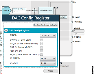 Figure 10. AD5423 DAC Confif Register Pop-Up Menu
Writing to the ADC Configuration Register
The procedure to set up and configure the ADC input node is discussed in the AD5423 data sheet. For this reason, writing to the ADC configuration register through the Apply Changes function is disabled.
The dropdown list in the SEQUENCE_COMMAND pane contains only an initiate single conversion command (INITIATE_SINGLE_CON). The hexadecimal text field in the SEQUENCE_DATA pane is unused and remains at 0. The dropdown list in the ADC_IP_SELECT pane is used to select the desired input node for the ADC to convert. Click Configure ADC to initiate a write to the ADC configuration register. A register read must be performed to see the ADC result in the status register (see Figure 11).
 Figure 11. AD5423 ADC Configuration Register
Updating Diagnostic Results
The AD5423 has a digital diagnostic results register and an analog diagnostic results register, which contain error flags for the on-chip digital and analog diagnostic features. Writing 1 to the respective error flags updates the error flag status.
To update the digital and analog diagnostic result registers, click Update and Readback. This button initiates the writing of a 1 to the selected error flag and then reads back the updated diagnostic result. Figure 12 shows the digital diagnostic results register. Figure 13 shows the analog diagnostic results register.
 Figure 12.
  Figure 13.
 Example Configuration Sequences
Several example configuration sequences are available. Click Example Sequences, and the window shown in Figure 14 appears. To enable any of the sequences, click the relevant sequence button, as shown in Figure 15. The sequence runs immediately and the output changes accordingly. To return to the main window, click Back to AD5423.
 Figure 14. Example Sequences Window
 Figure 15. Selecting an Example Sequence
ACE Tool Views
The ACE software provides additional functionality to the main view described in this user guide. Open these views from the View menu on the application toolbar. The ACE software features a macro tool, a register debugger tool, and an events tool.
Macro Tool
The macro tool records and saves commands as an ACE macro file. This feature is useful when sharing macros with other users to perform the same task multiple times. The user can import and run an ACE macro file.
Register Debugger Tool
Use the register debugger tool to perform raw writes to and reads from the device. The register debugger affects only the hardware and does not write to the memory map of the ACE software.
Events Tool
The events tool view contains a list of errors, warnings, and information messages generated within the application software.
Evaluation Board Schematic and Artwork
 Figure 16. EVAL-ADG5401FSDZ Supplies and Reference Options Schematic
 Figure 17. SDP-S
Board Connections, Address Pins, and /LDAC and /RESET Pins Schematic
Figure 17. SDP-S
Board Connections, Address Pins, and /LDAC and /RESET Pins Schematic
 Figure 18. ADP1301-1 PMU Schematic
 Figure 19. AD5423 Schematic
 Figure 20. ADG5401F Schematic
 Figure 21. EVAL-ADG5401FSDZ Silkscreen
 Figure 22. EVAL-ADG5401FSDZ Primary Layer, Top Layer
 Figure 23. EVAL-ADG5401FSDZ Ground Planes, Layer 2
 Figure 24. EVAL-ADG5401FSDZ Ground and Power Planes, Layer 3
 Figure 25. EVAL-ADG5401FSDZ Secondary Layer, Bottom Layer
Ordering Information
Bill of Materials
Table 5. Bill of Materials
| Reference Designator | Description | Manufacturer | Part Number |
|---|---|---|---|
| #FAULT_, #LDAC_, #RESET_, #SCLK_, #SDI_, #SDO_, #SYNC_, +VSENSE, -VSENSE, /FAULT_, /LDAC_, /RESET_, /SYNC_, CHART, PWRGD_, SCLK_, SDI_, SDO_, VIOUT, VSOURCE | Test point, green | Vero Technologies | 20-313138 |
| +3.3V_, ADR_REF_, AVDD1, AVDD2, AVSS, PVIN, REFIN_, REFOUT_, VLDO_ | Test point, red | Vero Technologies | 20-313137 |
| AGND1, AGND2, AGND3, AGND4, AGND5, DGND1, DGND2, DGND3, PGND1, PGND2 | Test point, black | Vero Technologies | 20-2137 |
| C1, C3 | Multilayer ceramic capacitor (MLCC), X7S | TDK | CGA6M3X7S2A475K200AB |
| C2, C4, C6, C11, C12, C13 | Capacitor, ceramic, X5R | Taiyo Yuden | LMK105BJ104KV-F |
| C14, C15, C16 | Capacitor, ceramic, X7R | TDK | CGA2B3X7R1H104K050BB |
| C19 | Capacitor, ceramic, X7R | Yageo | CC0603KRX7R9BB103 |
| C20, C22, C23, C24 | Capacitor, ceramic, X7R | AVX | 0603YC105KAT2A |
| C25 | Capacitor, ceramic, X7R, 1206 | AVX | 12065C154KAT2A |
| C26 | Capacitor, ceramic, X7R, 1206 | AVX | 12065C473JAT2A |
| C5, C7, C9 | Capacitor, ceramic, X7R, general-purpose | Murata | GRM21BZ71H475KE15L |
| C8 | Capacitor, ceramic, X6S, general-purpose | Murata | GRM188C81C475KE11D |
| D1 | Diode, Schottky, rectifier, SMD | Diodes Incorporated | BAT46W-7-F |
| D4 | Diode, Schottky, small signal | STMicroelectronics | BAT54KFILM |
| DS1, DS4, DS5 | LED, SMD, 0603, red | Vishay | TLMS1000-GS08 |
| DS2 | LED, SMD, 0603, green | Lumex | SML-LX0603GW-TR |
| EXT+3.3V_, PVIN_ | Connector, printed circuit board (PCB), two position terminal block header, single-row, 5.08 mm pitch | Phoenix Contact | 1757242 |
| JP1, JP2 JP3, JP4, JP5, JP7, JP8, JP9, JP10, JP12, JP18 | Connector, PCB, three position, male, header, unshrouded, single-row, 2.54 mm pitch | Harwin | M20-9990345 |
| JP11, JP13, JP14, JP15, JP16, JP17 | Connector, PCB, BERG, male, two position, single-row, M000385 | Amphenol | 69157-102 |
| L1, L3 | Inductor, shielded power, 12.25 Ω dc resistance, 0.135 A | Coilcraft Inc. | XFL2006-104MEB |
| P10 | Vertical type receptacle for SDP breakout board | Hirose | FX8-120S-SV(21) |
| P2_ | Connector, PCB, header, square post, straight, dual-row | Samtec | TSW-108-14-T-D |
| P3 | Terminal block, five position, green | Phoenix Contact | 1727049 |
| P4, P5 | Connector, PCB, pin socket | Vero Technologies | 66-3472 |
| R1, R10, R13, R30, R44, R45, R46, R49, R50, R51 | Resistor, thick film, chip | Multicomp | MC0063W060311K |
| R15, R16, R20, R31, R33, R34 | Resistor, thick film, chip | Multicomp | MC0063W06031100K |
| R2 | Resistor, precision, thick film, chip, R1206 | Panasonic | ERJ-8ENF1004V |
| R3 | Resistor, precision, thick film, chip | Panasonic | ERJ-6ENF2103V |
| R4 | Resistor, precision, thick film, chip | Panasonic | ERJ-1GNF1003C |
| R41, R42 | Resistor, chip, SMD | Vishay | CRCW06030000Z0EA |
| R5 | Resistor, precision, thick film, 0603 | Panasonic | ERJ-3EKF5903V |
| R6 | Resistor, precision, thick film, R0603 | Panasonic | ERJ-3EKF1822V |
| R7 | Resistor, film, SMD, 0603 | Multicomp | MC0063W0603139K |
| R8 | Resistor, thick film, chip | Vishay | CRCW0603715KFKEA |
| R9 | Resistor, thin film, precision | TE Connectivity | RN73C1J13K7BTG |
| S2 | Switch, tiny, washable, toggle switches | Apem Components | TL39P0050 |
| T1 | Flyback transformer, EPX6, SMT | Wurth Elektronik | 750316743 |
| U1 | Three-channel, isolated micropower management unit, seven digital isolators | Analog Devices | ADP1031ACPZ-1 |
| U2 | IC, 32 kb serial EEPROM | Microchip Technology | 24LC32A/SN |
| U4 | Ultralow noise, high accuracy voltage reference | Analog Devices | ADR4525BRZ |
| U5 | 16-bit, current and voltage output DAC, dynamic power control, HART connectivity | Analog Devices | AD5423BCPZ-REEL |
| U6 | Fault Protection, 6 Ω RON, SPST switch with 0.6 kΩ feedback channel | Analog Devices | ADG5401F |
Table 6. Bill of Materials (Uninserted Components)
| Reference Designator | Description | Manufacturer | Part Number |
|---|---|---|---|
| C18 | Capacitor, ceramic, X7R | Yageo | CC0603KRX7R9BB103 |
| C27 | Capacitor, ceramic, X7R, general-purpose | Murata | GRM188R71A225KE15D |
| P8, P9 | Connector, PCB, pin socket | Vero Technologies | 66-3472 |
| R12 | Resistor, thin-film, chip, high reliability | Panasonic | ERA-6AEB202V |
| R32, R35 | Resistor, thick film, chip | Multicomp | MC0063W06031100K |
| R36 | Resistor, precision, thick film, chip | Panasonic | ERJ-6ENF2000V |
| D2 | Diode, TVS, bidirectional | STMicroelectronics | SMAJ33CA-TR |
| E1, E2 | Murata | Ferrite Beads, 1 kΩ at 100 MHz | BLM41PG102SN1L |
| L4, L5 | Inductor, SMD | Bourns | CM453232-101KL |
resources/eval/adg5401fsdz.txt · Last modified: 04 Jun 2021 04:50 by Mar Christian Lacida