


The most recent version of this page is a draft. This version is outdated by a newer approved version.This version (28 Mar 2013 19:35) was approved by David Brandon.The Previously approved version (28 Mar 2013 19:02) is available.
This version is outdated by a newer approved version.This version (28 Mar 2013 19:35) was approved by David Brandon.The Previously approved version (28 Mar 2013 19:02) is available.This is an old revision of the document!
Table of Contents
AD9914 Evaluation Board User Guide
GENERAL DESCRIPTION
This user guide describes how to set up and use the AD9914 evaluation board. The AD9914 is a 3.5 GSPS direct digital synthesizer (DDS) with a 12-bit DAC. The evaluation board software provides a graphical user interface (GUI) for easy communication with the device along with many user friendly features, such as the mouse-over effect. This user guide is intended for use in conjunction with the AD9914 data sheet.

FIGURE 1. AD9914/PCBZ
FEATURES
- PC evaluation software for control and measurement of the AD9914
- USB connection to PC
- Microsoft Windows-based evaluation software with simple graphical user interface(supports 64-bit versions of Windows)
APPLICATIONS
- Agile LO frequency synthesis
- Programmable clock generator
- FM chirp source for radar and scanning systems
- Test and Measurement equipment
- Acousto-optic device drivers
- Polar modulator
- Fast frequency hopping
EVALUATION BOARD SOFTWARE
The AD9914 evaluation software allows the user to control the full functionality of the AD9914 through SPI communication on the evaluation board. 64-bit versions of Windows® are supported. Use the following instructions to set up the evaluation board software.
Software Installation
Do not connect the evaluation board until the software installation is complete.
- Uninstall any prior versions of the software before a new installation update.
- Administrative privileges are required for installation.
- Go to the ADI website to download the latest evaluation software http://www.analog.com/en/digital-to-analog-converters/direct-digital-synthesis-dds/ad9914/products/EVAL-AD9914/eb.html.
- Click on Software and Tools button and then click AD9914 Evaluation Board Software to download. The current version of software is AD9914_Setup_v1.0.4595.26695.exe. (Note that the website may have a newer version.) Follow the installation instructions as prompted.
Installing the Device Driver
After the installation of the evaluation software is complete, follow these steps to install the device driver:
- Power up the evaluation board and apply the REF CLK source. See the Evaluation board hardware section under for properly powering the evaluation board.
- Connect the evaluation board to the computer via the USB port using the USB cable included in the evaluation board kit. When the USB connection is recognized, a green LED light (D200) illuminates and the Found New Hardware Wizard dialog box appears.)
- Click Next to continue the installation of a new driver.
- Click Continue Anyway when the Hardware Installation Warning window appears.
- Click Finish in the Found New Hardware Wizard when installation is complete.
- Note, a second Found New Hardware Wizard dialog box usually appears again to complete the device driver installation. Repeat Step 3 to Step 5 in the Installing the Device Driver section.
Confirming the USB CONNECTION
A successful connection of the software to the board is indicated by a green USB icon, which can be found at the bottom right corner of the main GUI window.
Troubleshooting an Unsuccessful USB Connection
An unsuccessful connection is indicated by a flashing red USB icon located at the bottom right corner of the window. Most installation errors can be resolved by checking jumper settings, making sure that the evaluation board is powered up correctly, and inspecting the USB port and cable connections. When all power, USB port/cable connections, and jumper settings are correct, an error may still appear if the clock input is not configured properly. Check to make sure that the clock input source is connected and configured properly. Another reason an error may appear is due to the presence of a conflicting device driver. To resolve this issue, update the driver by plugging the USB connector into another USB port. When the Found New Hardware Wizard appears, install a device driver as follows:
- Select Install from a list or specific location (Advanced), and then click Next.

Figure 1. New Found Hardware Window - Choose Don’t search. I will choose the driver to install, and then click Next.

Figure 2. Search and Installation Options Window - Select the AD9914 Firmware Loader, and then click Next. Note that sometimes the operating system might load the wrong driver because the operating system detects multiple drivers, such as the evaluation board, that can be used by the hardware. In such a case, multiple drivers might be listed in this window. Select only the AD9914 Firmware Loader, and then click Next. A Hardware Installation box then appears. Click Continue Anyway, and then close the wizard by clicking Finish.

Figure 3. Select Device Driver Window
EVALUATION BOARD HARDWARE
The evaluation board provides all of the support circuitry required to operate the AD9914 in its various modes and configurations. Figure 1 shows the typical bench characterization connections used to evaluate the ac performance.
POWER SUPPLIES
The AD9914 evaluation board has one power supply connector labeled P300 to power the USB interface circuitry and the AD9914. This connector has four pins that the user must connect individual wires back to power supplies to power the AD9914 evaluation board. Table 1 shows the necessary connections and the appropriate supply voltage
| Pin | Label | Voltage |
|---|---|---|
| 1, 3 | GND | 0 |
| 2 | 3.3V | 3.3 |
| 4 | 1.8V | 1.8 |
Table 1. Power Supply Connections
INPUT REFERENCE CLOCK SIGNAL
The AD9914 architecture provides the user with two options when providing an input clock signal to the part: • Connect a high frequency input clock signal up to 3.5GHz to J104. • Connect a lower input reference frequency to J104 and enable the internal clock multiplier (PLL). The max frequency rate of the PFD of the internal PLL is 125MHz. The input clock to the DDS is called the REF CLK. The internal system clock runs at the REF CLK rate if the internal REF CLK multiplier (PLL) is disabled. Else the internal system clock runs at the output frequency rate of the PLL. Note: The input clock path on the AD9914 evaluation board uses an ADCLK925 clock buffer to drive the AD9914 differentially. Therefore, if the input signal into the ADCLK925 has a slow slew rate, the in-close phase noise performance of the AD9914 may be dramatically limited by the ADCLK925. Refer to the ADCLK925 data sheet for details on the maximum input speeds and input sensitivities. The SYNC_CLK runs at 1/24th the system clock rate and the default state is SYNC_CLK enabled. So, if the SYNC_CLK is not running, the device is powered down or the REF CLK is invalid.
DAC OUTPUT SIGNAL
The main output signal of the DDS is the DAC output. Note, the output of the DDS may or may not have a DAC reconstruction filter after the balun on the evaluation board depending on the revision of the board.
JUMPER SETTINGS
The jumpers on the AD9914 evaluation board are factory set so that the board is ready to use with PC control. The AD9914 software GUI operates the evaluation board in a serial interface only; however, you can also opt to use an alternative external control. Table 2 lists the jumper settings used for PC control and external control. Note that this document does not cover all aspects of externally controlling the AD9914 evaluation board.
Note, if you tri-state the USB circuitry to drive the board externally, you must control all those tri-stated inputs to the AD9914, else the device may not response to external stimulus. For example, if the master reset input or the EXT_PWR_DWN input are floating any external programming would have intermittent issues. All AD9914 digital inputs are accessible via the provided header connectors.
| Mode | Settings |
|---|---|
| PC Control (Factory Settings) | 1) Set Jumpers P203, P204, P205 to Enable |
| 2) Install Jumpers P105, P202, P205 to Enable | |
| 3) Set Jumpers IOCFG0 to IOCFG4 to 1000 | |
| External Control | 1) Set Jumpers P203, P204, P205 to Disable |
| 2) Control the AD9914 via External Header Connnectors |
Table 2. Jumper Settings for Communication Modes
EXTERNAL HEADER CONNECTORS
The external I/O control headers provide a parallel or serial communication interface for the AD9914 when the part is under the command of an external controller. In addition, the headers provide an interface for modulation data depending on the setting of the function pins. See the AD9914 data sheet for more details on the function pins settings.
Disabling software GUI Control
Disabling the ICs on the evaluation board allows operating the board with an external serial or parallel control by configuring each buffer in its high imped¬ance state by its nearby jumper.
USB PORT
When the part is under PC control (default mode), the evaluation board communicates with the AD9914 via the USB port.
MODES OF OPERATION
PROFILE MODE
In profile mode, the three DDS signal control parameters (frequency, phase offset, and amplitude scaling) are supplied directly from 1 of 8 internal profile registers. A profile is an independent register that contains all three control parameters. You can use a profile register to output a single tone frequency or use multiple pre-program profile registers and the profile pins to hop between frequencies, phase offsets and/or different amplitude settings. The following example are the steps to program a single profile to output a single tone frequency using the AD9914 software GUI.
Single-Tone Operation
- Power up the AD9914 evaluation board and apply the REF CLK source to clock the AD9914.
- Launch the AD9914 evaluation software. After the software recongnizes the evaluation board, click the Master Reset ICON button in the main tool bar of the software GUI (labeled 1 in Figure 6). The Master Reset clears all memory elements and sets registers to default values.
- Enter the desired REF CLK frequency value in the External Clock box. If the internal PLL is to be used, enable and load those desired PLL settings at this time.
- After the desired system clock frequency appears in the main tool bar of the software GUI, click the DAC Calibration ICON button (labeled 3 in Figure 6). The DAC CAL is required once for the initial setup and/or every time the REF CLK frequency is changed.
- Click the Profiles tab to access the Profiles window and enable profile mode via check box
- Enter the desired output frequency in Profile 0. See figure 2 below for a view of an individual profile.
- Click the flashing Load button (labeled 5 in Figure 6) near the top of the GUI.
- At this time you can view the DAC output single tone frequency performance via an oscilloscope or spectrum analyzer.
To select a profile other than Profile 0, use the Selected profile drop-down menu. NOTE: Unfortunately, the profile pin signals are sent asynchronously from the buffer ICs on the evaluation board to the AD9914 profile pins. So, it's possible the profile selected may not go to the desired profile selected because the profile signals are not synchronous to the SYNC_CLK. If the selected profile setting does not point to the correct profile settings chosen, sending an IO_UPDATE or clicking the LOAD button will correct this issue. This would not be an issue if the profile signals were sychrnonously transmitted to the AD9914.
Profile Data Entry

Figure 4. Single Profile Window
The Frequency box is used to set the frequency generated by the DDS. The input values are in megahertz (refer to AD9914 data sheet for the acceptable range of output frequencies).
The Phase Offset box controls the phase of the DDS output. The input is in degrees and can be changed from 0° to 360° with 16-bit resolution.
The Amplitude Scale Factor box digitally controls the amplitude of the carrier from the DDS. This scalar ranges from 0 to 1 and has a 12-bit resolution. Note that this function works only if the OSK enable is selected in the Control tab.
Note that Frequency, Phase Offset, and Amplitude Scale Factor can accept native data that are going to be loaded directly to the registers. This data is binary in form but can also be expressed as hexadecimal or decimal. Change the format by clicking the drop-down button to the right side of each box.
SWEEP MODE
The Digital Ramp Generator (DRG) window is accessible via the Sweep Tab directly below the GUI tool bar. The DRG can sweep frequency, phase, or amplitude. The DRG allows independent control of the slope of a rising sweep and the falling sweep along with other features. See figure below for Digital Ramp Generator window.
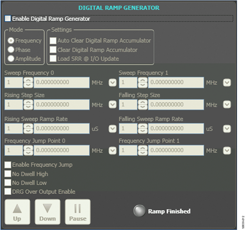
Figure 5. Digital Ramp Generator Window
To enable the DRG for configuration, select the Enable Digital Ramp Generator check box. In the Mode section, select the parameter (frequency, Phase, or Amplitude) to be sweeped. In the Settings section, the Auto Clear Digital Ramp Accumulator check box allows the DRG to be cleared every time the I/O update signal is applied or when there is a profile pin change. The Clear Digital Ramp Accumulator check box will keep the DRG cleared until the check box is cleared. The Load SRR @ I/O Update check box allows the reload of a new digital ramp rate when an I/O update is issued or when there is a profile change.
If the parameter to be sweeped is frequency, use the Sweep Frequency 0 and Sweep Frequency 1 boxes to enter the lower frequency limit value and upper frequency limit value, respectively. The units are megahertz for freqency, degrees for phase and Volts for amplitude. Note, the value in the Sweep 0 box is required to be be less than the value in the Sweep 1 box regardless of the parameter being swept. The Rising Sweep Ramp Rate and Falling Sweep Ramp Rate boxes are used to set the time between each rising or falling step on the ramp and is in units of microseconds.
The No Dwell High and No Dwell Low check boxes are used to instantaneously return to the lower or upper limit depending of which box is checked. To continously repeat a parameter sweep without clicking the up/down buttons or just enable both No Dwell bits. If not, use the Up, Down, and Pause buttons at the bottom of the window to control the sweep direction or to halt the sweep. The Ramp Finished indicator illuminates when the ramp is complete.
NOTES:
- The rising and falling ramp rate windows in the present version of software are reversed. This will be addressed in a software revision. For now make the appropriate changes.
- If the DRG is used to sweep amplitude, the OSK enable bit must be selected in the Control tab window.
- After the desired configuration is completed saving the setup is preformed using the save settings feature.
PROGRAMMABLE MODULUS MODE
Programmable Modulus Window
The chip is in programmable modulus mode when the Enable Programmable Modulus check box is selected. Note, the digital ramp generator mode is automatically disabled.
The Programmable Modulus window is used to alter the frequency equation of the DDS core, making it possible to implement fractions that are not restricted to a power of 2 in the denominator.
When you enter the desired output frequency (in megahertz) in the Fout box, the values in the Register Values boxes and the Divide Ratio boxes are automatically updated. You can also directly input a divide ratio, which in turn automatically updates the Register Values boxes and the Output Frequency box.
OVERVIEW OF THE GUI WINDOWS
Toolbar
The toolbar near the top of the evaluation software main window includes several buttons, each labeled with an icon, that allow you to easily initiate various actions (please refer to Figure 6 for a detailed description and the requirements of each toolbar element).

Figure 6. Toolbar Description
Tabs
There are five tabs available in the main window of the evaluation software: Control, Profiles, Sweep, Modulus, and Debug. The following tab descriptions provide a brief overview of each tab; more detailed information can be found in the Evaluation and Test section.
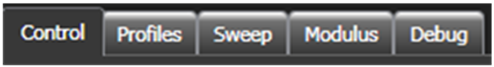
Control Tab
The Control tab provides control of the internal PLL, parallel port, auxiliary functions, I/O control, power-down functions, output shift keying (OSK), clock calibration, and multichip sync function of the AD9914 (see Figure 8).
Profiles Tab
The Profiles tab allows enabling the profile mode, in which the DDS signal control parameters are supplied directly from the profile programming registers. A profile is an independent register that contains the DDS signal control parameters.
NOTE: Unfortunately it is not a guaranteed selecting a profile above will switch to the correct profile setting. The reason, the profile signals are sent asynchronously via the GUI hardware. The reality is the profile signals need to meet setup and hold times to the SYNC_CLK.
Sweep Tab
Digital ramp generator (DRG) is synonymous with linear sweep. The ramp generation parameters in the Sweep tab allow you to control both the rising and falling slopes of the ramp, the upper and lower boundaries of the ramp, the step size and step rate of the rising portion of the ramp, and the step size and step rate of the falling portion of the ramp. This is digitally generated with a 32-bit output resolution that can be programmed to represent frequency, phase, or amplitude. Refer to AD9914 data sheet for more information on DRG.
Modulus Tab
The Modulus tab allows you to enable programmable modulus mode and to alter the frequency equation of the DDS core, making it possible to implement fractions that are not restricted to a power of 2 in the denominator. See the data sheet for more details.
Debug Tab
The Debug tab provides complete direct access to the register map as well as control of many external pins. The Debug tab is intended for debugging issues with the AD9914. Although this tab can be used for all programming, it is not user friendly for programming purposes and, therefore, using the Debug tab for purposes other than debugging may result in improper programming of reserved bits.
resources/eval/ad9914-user-guide.1364495697.txt.gz · Last modified: 28 Mar 2013 19:34 by David Brandon