


This version (13 Jan 2023 02:54) was approved by John Xavier Toledo.The Previously approved version (17 Nov 2022 03:17) is available.
Table of Contents
EVALUATING THE AD9684 ANALOG-TO-DIGITAL CONVERTER
Preface
This user guide describes the AD9684 evaluation board which provides all of the support circuitry required to operate the ADC in its various modes and configurations. The application software used to interface with the devices is also described.
The AD9684 data sheet provides additional information and should be consulted when using the evaluation board. All documents and software tools are available at www.analog.com/hsadcevalboard. For additional information or questions, send an email to highspeed.converters@analog.com.
AD9684 Evaluation Board
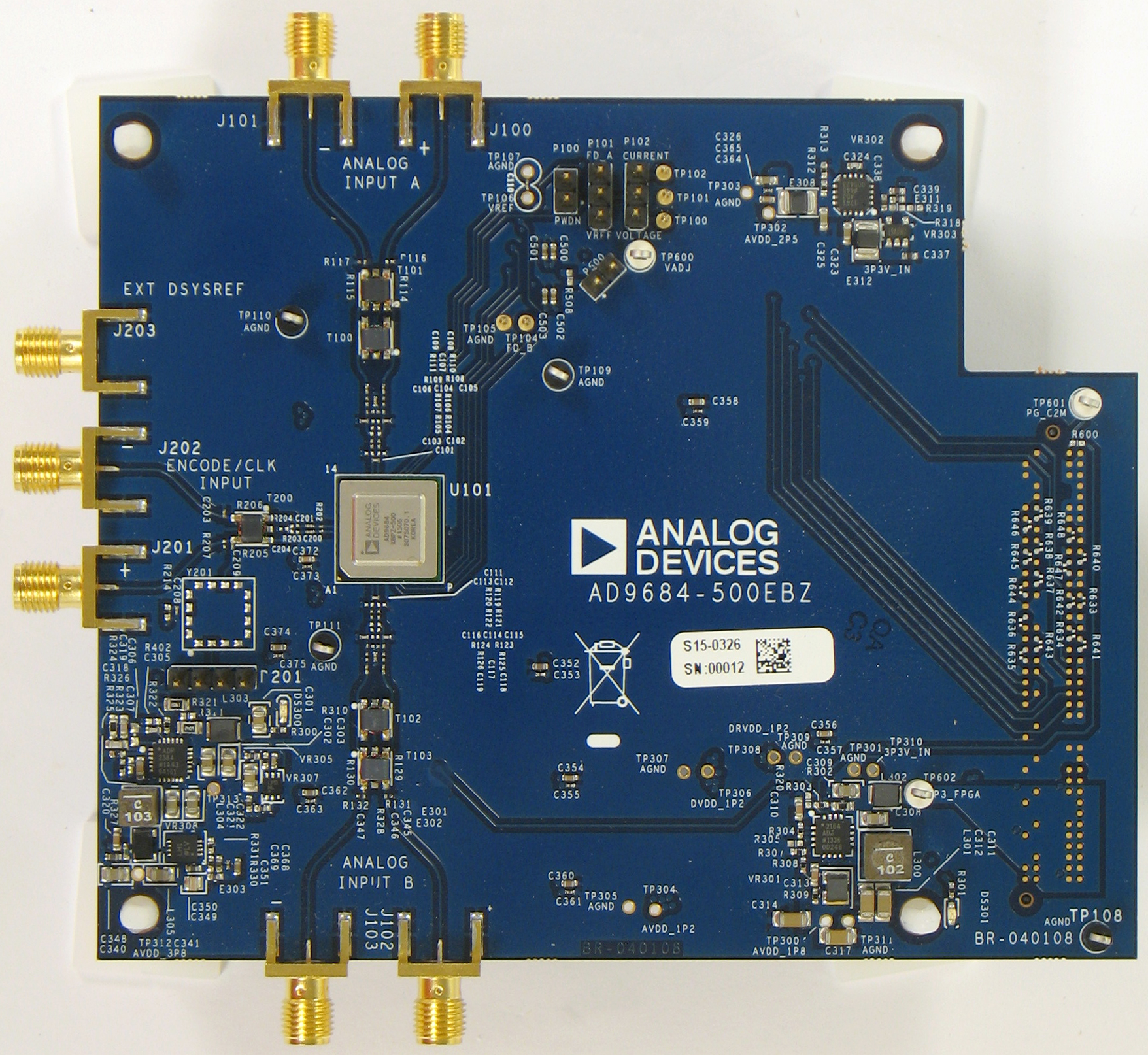
Figure 1. AD9684 Evaluation Board
Typical Measurement Setup
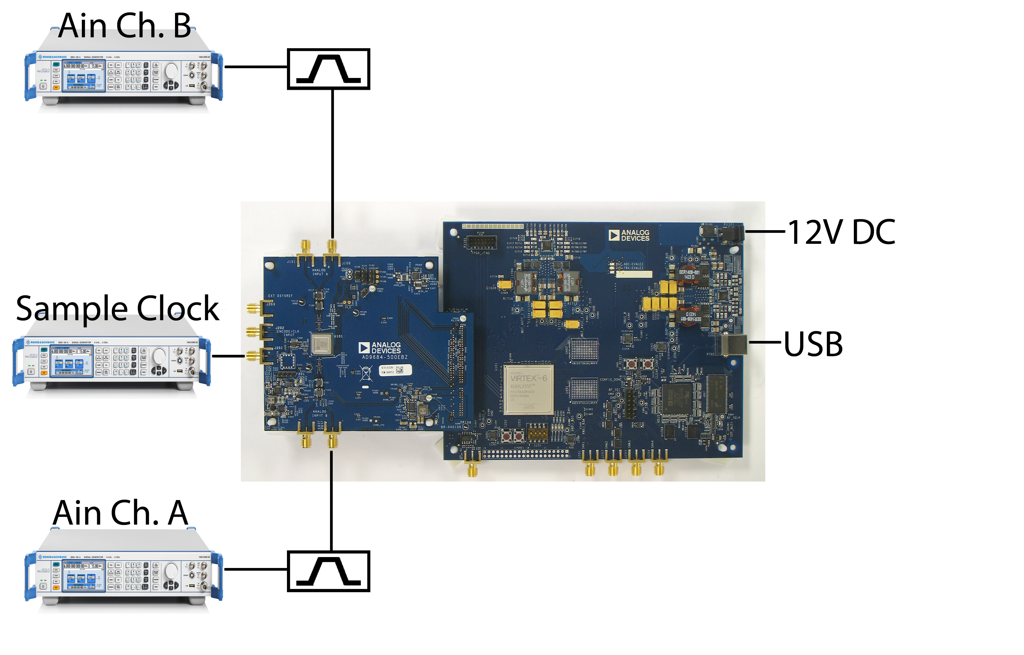
Figure 2. Evaluation Board Connection—AD9684-500EBZ (on Left) and HSC-ADC-EVALEZ (on Right)
Features
- Full featured evaluation board for the AD9684
- SPI interface for setup and control
- Wide band Balun driven input
- No external supply needed. Uses 12V-1A and 3.3V-3A supplies from FMC
- VisualAnalog® and SPI controller software interfaces
Helpful Documents
- AD9684 Data Sheet
- HSC-ADC-EVALEZ, HSC-ADC-EVALEZ Evaluation Kit
- AN-905 Application Note, VisualAnalog Converter Evaluation Tool Version 1.0 User Manual
- AN-878 Application Note, High Speed ADC SPI Control Software
- AN-877 Application Note, Interface to High-Speed ADCs via SPI
- AN-835 Application Note, Understanding ADC Testing and Evaluation
Software Needed
Design and Integration Files
- Schematic: AD9684 Rev A
- Layout: AD9684 Rev A
- Bill of Materials: AD9684 Rev A
- FPGA MCS file: ad9684_evalez_05202014_0903am.zip
Equipment Needed
- Analog signal source and antialiasing filter
- Encode clock source
- 12V, 6.5A switching power supply (such as the SL POWER CENB1080A1251F01 supplied with HSC-ADC-EVALEZ)
- PC running Windows®
- USB 2.0 port
- AD9684-500EBZ board
- HSC-ADC-EVALEZ FPGA-based data capture kit
Getting Started
This section provides quick start procedures for using the evaluation board for AD9684.
Configuring the Board
Before using the software for testing, configure the evaluation board as follows:
- Connect the evaluation board to the HSC-ADC-EVALEZ data capture board, as shown in Figure 2.
- Connect one 12V, 6.5A switching power supply (such as the CENB1080A1251F01 supplied) to P4 on the HSC-ADC-EVALEZ board. Connect the Standard-B USB port of the HSC-ADC-EVALEZ board to the PC with the supplied USB cable.
- Turn on the HSC-ADC-EVALEZ.
- The HSC-ADC-EVALEZ will appear in the Windows(R) Device Manager
- If the Device Manager does not show the HSC-ADC-EVALEZ listed as shown in Figure 2, unplug all USB devices from the PC, uninstall and re-install SPIController and VisualAnalog and restart the hardware setup from step 1.
- On the ADC evaluation board, provide a clean, low jitter 1GHz clock source to connector J201 and set the amplitude to 14dBm. This is the ADC Sample Clock.
- On the ADC evaluation board, use a clean signal generator with low phase noise to provide an input signal for channel A to J100. Use a shielded, RG-58, 50 Ω coaxial cable to connect the signal generator output to the ADC Evaluation Board. For best results, use a narrow-band, band-pass filter with 50 Ω terminations and an appropriate center frequency. (ADI uses TTE, Allen Avionics, and K & L band-pass filters.)
- On the ADC evaluation board, use a clean signal generator with low phase noise to provide an input signal for channel B to J102. Use a shielded, RG-58, 50 Ω coaxial cable to connect the signal generator output to the ADC Evaluation Board. For best results, use a narrow-band, band-pass filter with 50 Ω terminations and an appropriate center frequency. (ADI uses TTE, Allen Avionics, and K & L band-pass filters.)
Visual Analog Setup
- Click Start
All Programs
- On the VisualAnalog “New Canvas” window, click ADC
- Select a Dual ADC
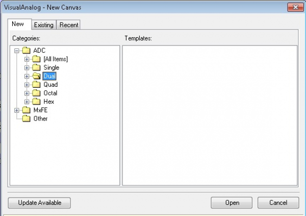
Figure 3. Selecting the AD9684 canvas
- Select the AD9684
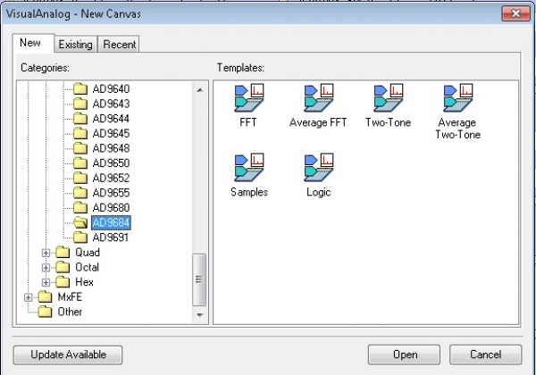
Figure 4. Selecting the AD9684 canvas
- View the AD9684 canvas
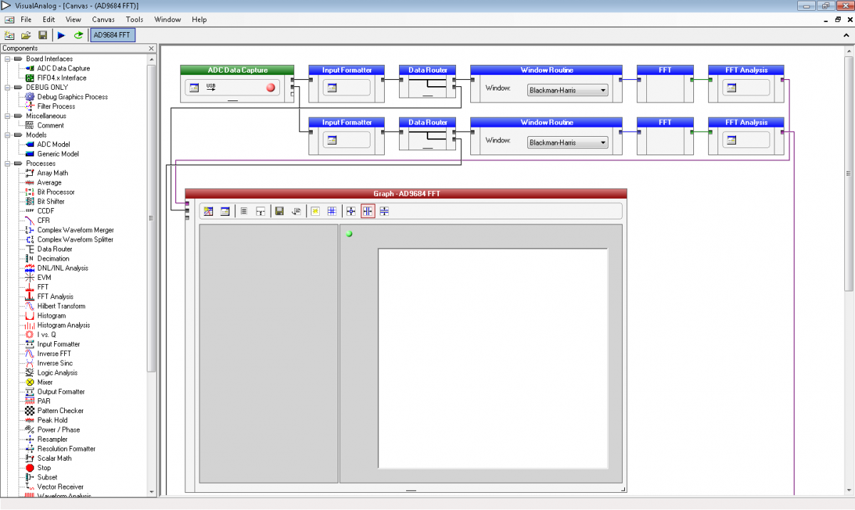
Figure 5. TheAD9684 canvas
- If VisualAnalog opens with a collapsed view, click on the “Expand Display” icon (see figure 6)

Figure 6. Expanding Display in VA
- Click the Settings button in the ADC Data Capture block to view the capture size as shown in Figure 7

Figure 7. Setting the capture length
- On the General tab make sure the clock frequency is set to 500MHz (or other clock frequency). The FFT capture length may be changed to 131072 (128k) per channel. The HSC-ADC-EVALEZ FPGA software supports up to 256K FFT capture (128K per channel)
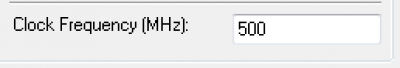
Figure 8. Setting the clock frequency
- Click on the Capture Board tab and browse to the ad9684_evalez_05202014_0903am.mcs file. Click the Program button. The FPGA_DONE LED should illuminate on the HSC-ADC-EVALEZ board indicating that the FPGA has been correctly programmed. The bin file is available at the Design and Integration Files section
- Click OK


SPIController Setup
- Click Start
- Select the appropriate configuration file when prompted.
- In the Global tab, under the Generic Read/Write section, write 0x81 to register 0x000. This issues a Soft reset for the DUT.
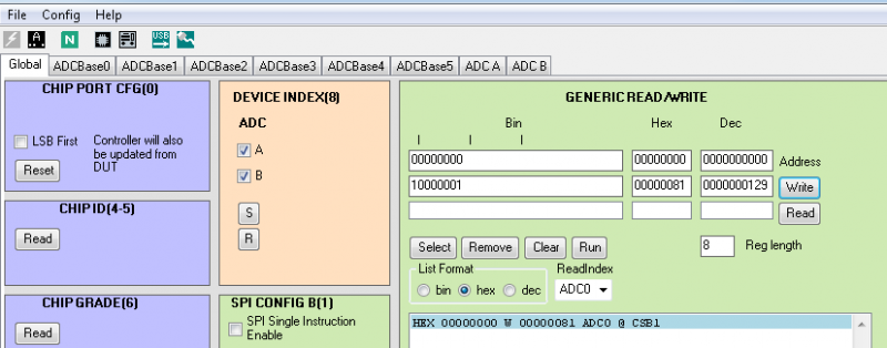
Figure 9. Sending a Soft Reset to the AD9684
- Individual Channel control for ADC A and ADC B are done using the Device Index Register (0x008) in the Global tab.

Figure 10. Device Index for ADC Channel A and Channel B
- Under ADC A and ADC B tabs the options for Channel A and B are listed. Default settings have been programmed to ensure optimal performance for the input bandwidth and sample rate. Only the following options need to be operated with:
- Chip Configuration Register (2): This option allows the channel to be powered on
- Buffer Current Setting (18): This option allows the buffer current to change to enable better harmonic performance at different frequencies. At high analog input frequencies, the buffer current may need to be increased to optimize harmonic distortion performance (HD2, HD3). Keep in mind that at high frequencies, the performance is also jitter limited. So increasing the buffer currents may lead to diminishing returns with higher power consumption. Refer to the datasheet to understand the relationship between IAVDD3 and Buffer Current Setting.
- Analog Input Differential Termination (16): This sets the input termination. Recommended settings are 400, 200, 100, 50 ohms. At lower termination settings, the harmonic distortion performance may show improvement, but the analog input signal amplitude will be reduced.
- Input Full Scale Range (25): At high input frequencies, in order to preserve the linearity of the input buffer, it may be beneficial to reduce the input full-scale range in order to get more harmonic distortion performance. This in turn may negatively affect the SNR of the ADC.

Device Setup - Full Bandwidth Mode
- The settings in the ADCBase0 tab must be changed to configure the AD9684. In this example, the AD9684 is set up to use Full Bandwidth Mode for 2 ADC channels. Set the Chip Application Mode in register 0x200 to Full Bandwidth Mode. Set the Chip Decimation Ratio in register 0x201 to Full Sample Rate. Since the chip is configured to Full Bandwidth mode, the DDC configuration is bypassed and the sampling frequency is decimated by 1.

Figure 11. Set Application Mode to Full Bandwidth Mode

Obtaining an FFT - Full Bandwidth Mode
- The first item to configure in Visual Analog is the input clock frequency. This is the frequency of the input clock and NOT the decimated sample rate (if using decimation). Click in the ADC Data Capture block to open the settings. In this example, 500MHz is the input clock frequency.
- Click the Run button in Visual Analog and you should see the capture data similar to the plot below.
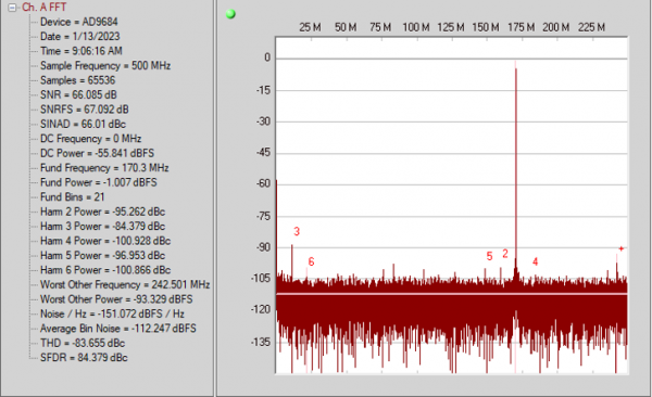
Figure 12. AD9684-500 FFT at 170.3 MHz Input signal for Full Bandwidth Mode
- Adjust the amplitude of the input signal so that the fundamental is at the -1.0 dBFS level. (Examine the Fund Power reading in the left panel of the VisualAnalog FFT window.)
- To save the FFT plot do the following:
- Click on the Float Form button in the FFT window
Figure 13. Floating the FFT window
- Click on File
Figure 14. Saving the FFT


Device Setup - 2 ADCs, 2DDCs, Real Mode Decimate by 2
- The settings in the ADCBase0 tab must be changed to configure the AD9684 to use the DDCs. In this example the AD9684 is set up to use two DDCs (one per ADC channel) with real outputs and a decimation ratio of two. Set the Chip Application Mode in register 0x200 to Two Digital Down Converters and select the Only Real (I) Selected checkbox. Set the Chip Decimation Ratio in register 0x201 to Decimate by 2 Ratio.
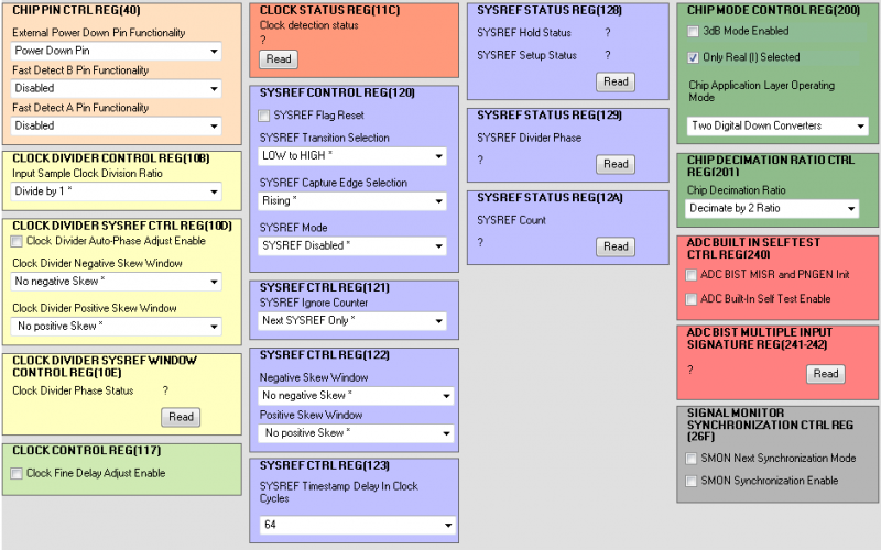
Figure 15. Set Application Mode to 2 DDCs Real Mode Decimate by 2
- The DDC settings must be configured in ADCBase1, but first, the tuning step, translation frequency, and DDC Phase Increment must be calculated.
- The tuning step is equal to the output sample rate divided by 4096.
- tuning step = 500MSPS/4096 = 122070.3125
- The translation frequency is equal to the output sample rate divided by 4*(decimation ratio).
- translation frequency = 500MSPS/(4*2) = 62500000
- The DDC Phase Increment is equal to the translation frequency divided by the tuning step.
- DDC Phase Increment = 62500000/122070.3125 = 512
- Under DDCO CTRL and DDC1 CTRL in the ADCBase1 tab configure the DDCs to select 6dB Gain, Decimate by 4 Filter Selection (when in real mode this actually sets the AD9684 to Decimate by 2), Real (I) Output Only, Both Input Sample Selections to Channel A for DDC0 and Channel B for DDC1, and the DDC Phase Increment to the calculated value of 512
- After changing DDC selections, perform a soft reset of the DDCs by checking and unchecking the box for DDC Soft Reset under the DDC Synchronization CTRL Reg (300).
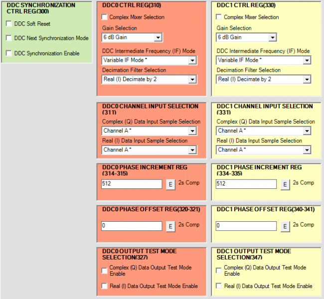
Figure 16. Channel A and Channel B DDC Settings


Obtaining an FFT - 2 ADCs, 2DDCs, Real Mode Decimate by 2
- The first item to configure in Visual Analog is the input clock frequency. This is the frequency of the input clock and NOT the decimated sample rate (if using decimation). Click in the ADC Data Capture block to open the settings. In this example, 500MHz is the input clock frequency. In addition, the DDC data must be selected under the Output Data section. DDC0 and DDC1 are being used in the AD9684 so this must be selected under the ADC Data Capture Settings.
- Click the Run button in Visual Analog and you should see the capture data similar to the plot below.

Figure 17. AD9684-500 FFT with 2 DDCs in Real Mode with Dec2 Enabled
- Adjust the amplitude of the input signal so that the fundamental is at the desired level. (Examine the Fund Power reading in the left panel of the VisualAnalog FFT window.) Real DDC operation imposes ~0.7 dB loss on the input signal but does not impact the dynamic range. A -1.0 dBFS input signal will show as -1.7 dBFS in the FFT in Visual Analog.
- To save the FFT plot do the following:
- Click on the Float Form button in the FFT window
Figure 18. Floating the FFT window
- Click on File
Figure 19. Saving the FFT

Device Setup - 2 ADCs, 1DDC, Complex ZIF Mode Decimate by 2
- The settings in the ADCBase0 tab must be changed to configure the AD9684 to use the DDC. In this example the AD9684 will be set up to use one DDCs with a complex ZIF output (NCO bypassed) and a decimation ration of two. Set the Chip Application Mode in register 0x200 to One Digital Down Converter and make sure the Only Real (I) Selected checkbox is NOT checked. Set the Chip Decimation Ratio in register 0x201 to Decimate by 2 Ratio.

Figure 20. Set Application Mode to 1 DDC Complex ZIF Mode Decimate by 2
- The DDC settings must be configured under DDC0 CTRL in the ADCBase1 tab configure the DDC to select Complex Mixer Selection, 0 Hz IF Mode, Decimate by 2 Filter Selection, Real (I) Input Sample Selection to Channel A for DDC0, and Complex (Q) Input Sample Selection to Channel B.
- After changing DDC selections, perform a soft reset of the DDCs by checking and unchecking the box for DDC Soft Reset under the DDC Synchronization CTRL Reg (300).
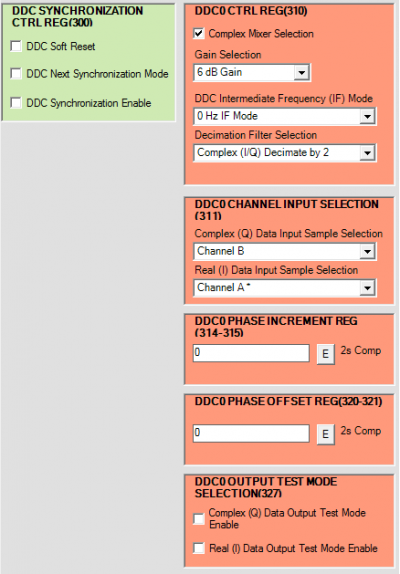
Figure 21. DDC Settings for Complex ZIF Mode


Obtaining an FFT - 2 ADCs, 1DDC, Complex ZIF Mode Decimate by 2
- The first item to configure in Visual Analog is the input clock frequency. This is the frequency of the input clock and NOT the decimated sample rate (if using decimation). Click in the ADC Data Capture block to open the settings. In this example, 500MHz is the input clock frequency. In addition, the DDC data must be selected under the Output Data section. DDC0 is being used in the AD9684 so this must be selected under the ADC Data Capture Settings.

Figure 22. AD9684-500 FFT Data Capture Settings
- In order to exclude the image frequency from the SFDR measurements, configure Visual Analog to remove the image from its calculations. This is done under the FFT Analysis settings. Under the User-Defined tab add a new row by clicking Add. Name it ‘Image’. Use a symbol such as the # and set the Freq to ‘-fund’. Set the Single-Side Band to 3 Bins and set it as ‘Spur, Exclude’. Once done, select the row, and then hit the Move Up button to place this new row just below the row with Fund.
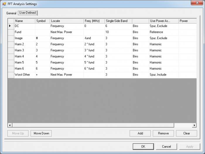
Figure 23. AD9684-500 FFT with 2 DDCs in Real Mode with Dec2 Enabled
- Click the Run button in Visual Analog and you should see the capture data similar to the plot below.
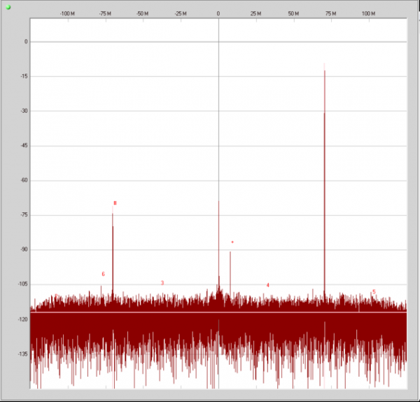
Figure 24. AD9684-500 FFT with 1 DDC in Complex ZIF Mode with Dec2 Enabled
- Adjust the amplitude of the input signal so that the fundamental is at the desired level. (Examine the “Fund Power” reading in the left panel of the VisualAnalog FFT window.) Complex DDC operation imposes ~1dB loss in the signal, but does not impact the dynamic range. A -1dBFS input signal will show as -2dBFS in Visual Analog.
- To save the FFT plot do the following
- Click on the Float Form button in the FFT window
Figure 25. Floating the FFT window
- Click on File
Figure 26. Saving the FFT


Troubleshooting Tips
FFT plot appears abnormal
- If you see a normal noise floor when you disconnect the signal generator from the analog input, be sure you are not overdriving the ADC. Reduce input level if necessary.
- In VisualAnalog, Click on the Settings button in the Input Formatter block. Check that Number Format is set to the correct encoding (twos compliment by default). Repeat for the other channel.
- Issue a Data Path Soft Reset through SPIController Global tab as shown in Figure 27
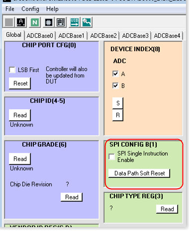
Figure 27. Issuing a data path soft reset through SPIController
The FFT plot appears normal, but performance is poor.
- Make sure you are using the appropriate band-pass filter on the analog input.
- Make sure the signal generators for the clock and the analog input are clean (low phase noise).
- If you are using non-coherent sampling, change the analog input frequency slightly, or use coherent frequencies.
- Make sure the SPI config file matches the product being evaluated.
The FFT window remains blank after the Run button is clicked
- Make sure the evaluation board is securely connected to the HSC-ADC-EVALEZ.
- Make sure the FPGA has been programmed by verifying that the Config DONE LED is illuminated on the HSC-ADC-EVALEZ. If this LED is not illuminated reprogram the FPGA through VisualAnalog. If the LED still does not illuminate disconnect the USB and power cord for 15 seconds. Connect again and repeat the hsc-adc-evale setup process.
- Make sure the correct FPGA bin file was used to program the FPGA.
- Be sure that the correct sample rate is programmed. Click on the Settings button in the ADC Data Capture block in VisualAnalog, and verify that the Clock Frequency is properly set.
- Restart SPIController.
VisualAnalog indicates that the “FIFO capture timed out” or “FIFO not ready for read back”
- Make sure all power and USB connections are secure.
VisualAnalog displays a blank FFT when the RUN button is clicked
- Ensure that the clock to the ADC is supplied. Using SPIController ADCBase0 tab the status of the clock can be read out. See figure 28.

Figure 28. Clock Detection Status Register

resources/eval/ad9684-500ebz.txt · Last modified: 13 Jan 2023 02:42 by John Xavier Toledo