


This version (03 Jan 2021 22:14) was approved by Robin Getz.The Previously approved version (30 Mar 2015 16:56) is available.
Table of Contents
AD9525 Evaluation Board User Guide
Features
- Simple power connection using 6 V wall adapter and on board LDO voltage regulators
- 6 ac-coupled differential LVPECL SMA connectors
- 2 single-ended LVPECL SMA connectors
- 1 LVPECL or 2 CMOS SMA connectors for sync output
- SMA connectors for:
- 3 reference inputs
- Charge pump output
- Clock distribution input
- USB connection to PC
- Microsoft Windows-based evaluation software with simple graphical user interface (supports 64-bit versions of Windows)
- On-board PLL loop filter
- Easy access to digital I/O and diagnostic signals via I/O header
- Status LEDs for diagnostic signals
Equipment Needed
- Reference oscillator or signal generator
- Other evaluation board to be clocked or test equipment
- Converters, DDS, transceivers
- Oscilloscope, spectrum analyzer, phase noise analyzer
- SMA cables (50 Ω)
- 6 V wall supply (provided)
- USB cable (provided)
Online Resources
GENERAL DESCRIPTION
The AD9525 evaluation board is a compact, easy to use platform for evaluating all features of the AD9525. Two versions of the evaluation board are available : one with a prepopulated external VCO and loop filter (AD9525/PCBZ-VCO) and one with no VCO/VCXO and no loop filter (AD9525/PCBZ). This user guide focuses on the AD9525/PCBZ-VCO, which already has a VCO and loop filter on board. The AD9525 provides a low power, multioutput, clock distribution function with low jitter performance, along with an on-chip PLL that can be used with an external VCO or VCXO. The VCO input and eight LVPECL outputs can operate up to a frequency of 3.6 GHz. All outputs share a common divider that can provide a division of 1 to 6. The AD9525 also offers a dedicated output that can be used to provide a programmable signal for resetting or synchronizing a data converter. For more information about the device, see the AD9525 data sheet. This user guide should be used in conjunction with the AD9525 data sheet and the software documentation available at www.analog.com/clocks

Figure 1. AD9525/PCBZ-VCO
EVALUATION BOARD HARDWARE
The instructions in this section are for setting up the physical connections to the AD9525/PCBZ-VCO evaluation board with a prepopulated VCO. There is another version of the evaluation board (AD9525/PCBZ) that does not contain an external VCO. The two variations of the evaluation boards have slightly different default configurations.
When connecting the evaluation board to a PC for the first time, you must install the evaluation software prior to connecting the evaluation board. If a previous version of the software is already installed, uninstall it before installing the latest version.
Power and PC Connections
- Install the AD9525 evaluation software, uninstall prior versions of the software before installation updates. Administrative privileges are required for installation. The 64-bit versions of Windows® are supported.
- Connect the 6V wall power supply to the main power connector labeled P500.
- Connect the USB cable to the evaluation board and the computer. The red LED labeled CR400 on the AD9525 evaluation board should illuminate.
- If the Found New Hardware Wizard window automatically appears when the evaluation board is connected, select Install the software automatically and click Next. The Found New Hardware Wizard window may appear twice, and a system restart may be required.
Refer to the Evaluation Board Software section for details on running the AD9525 evaluation board software.
Signal Connections
To connect signals:
- Connect a signal generator to the J202 (REF A) SMA connector or to the J204 (REF B) SMA connector. By default, the reference inputs on this evaluation board are ac-coupled and terminated 50 Ω to ground. An amplitude setting of 0 dBm to 6 dBm is sufficient.
- Connect an oscilloscope, spectrum analyzer, or other lab equipment to any of the J301 to J316 SMA clock OUT connectors on the edge of the board.
- OUT0 through OUT7 are ac-coupled LVPECL outputs terminated 150 Ω to ground.
- OUT3 and OUT6 contain a balun for differential to single-ended conversion. Connector J317 and J318 are for the SYNC_OUT distribution and are also ac-coupled LVPECL outputs terminated 150 Ω to ground.
- SYNC_OUT can be configured as two single-ended CMOS outputs, in which case each line should be terminated with a series resistor.
Bypassing the PLL (Clock Distribution Only)
To bypass the PLL:
- Connect a signal generator to the SMA connector labeled CLKIN.
- Remove C215.
- Install a 0 Ω resistor or ac coupling capacitor at R218. By default, this path contains a 6 dB T-type attenuator in between Connector J206 and the CLKIN pin.
The AD9525 default register settings configure the device as an eight output clock buffer.
Using An Off-Board VCO/VCXO
To use an off-board VCO or VCXO:
- Remove the original VCO/VCXO or disconnect all supply voltages. (You may see coupling between the VCO/VCXO paths if two VCO/VCXOs are powered at the same time, causing pulling.)
- Install a 0 Ω resistor at R217 and remove R225.
- Connect the external VCO/VCXO voltage tune input to J200 (CP_OUTPUT).
- Remove C215 and install a 0 Ω resistor or ac coupling capacitor at R218.
- Connect the off-board VCO/VCXO output to the J206 SMA connector (CLKIN).
- Design and populate a loop filter for the desired loop bandwidth and phase margin.
Note that the right angle SMA connectors on the evaluation board are not optimal for high speed signals. They are provided for ease of use but may cause loss of performance at speeds greater than 1.5 GHz.
LOOP FILTER DESIGN
The AD9525 PLL requires an external VCO or VCXO and a loop filter containing components tailored for a given application. The third-order passive configuration shown in Figure 2 usually results in the best performance for many applications and is the one found on the evaluation board.

Figure 2. PLL Loop Filter
The loop bandwidth of a PLL with a second-order filter (excluding R2 and C3) can be approximated using the following equation:
where:
- KVCO is the gain of the external VCO.
- ICP is the current of the charge pump.
- R1 is the resistance labeled in Figure 2.
- NTOTAL is the total of the feedback divider (set by a prescaler P, divider B, and divider M). Divider M only alters NTOTAL if the output frequency of the AD9525 is an integer division of the VCO frequency. NTOTAL is defined by the following equation:
Because KVCO is determined by the VCO vendor, the bandwidth of the loop can be adjusted by changing the values of ICP and NTOTAL. Note that ICP has a limited range, and NTOTAL is limited by the selectable values of Prescaler P, Divider B, and Divider M. For more information about NTOTAL and ICP, including possible values, see the AD9525 data sheet.
To determine the best loop filter for a given application, use ADIsimCLK™ (Version 1.5 or greater), which is free and can be downloaded from the ADIsimCLK Design and Evaluation Software Web page. This software aids in designing and exploring the capabilities and features of the AD9525, including designing the PLL loop filter.
The AD9525 evaluation board can be purchased with either a Z-Comm CRO2950B-LF external VCO or with no VCO populated. This section discusses a couple of different external VCO possibilities and their respective loop filter designs and performance. Using a high performance VCO with low phase noise allows you to create a low loop bandwidth filter to remove the jitter contained on the input reference clock.
Using the Evaluation Board with a Z-Comm CRO2950B-LF VCO
The first setup discussed is the default evaluation board configured with a Z-Comm CRO2950B-LF VCO. With the charge pump set to 1.8 mA and the feedback divider set to 24, the on-board loop filter produces a loop bandwidth of ~6 kHz and ~69° of phase margin. Table 1 shows the parameters used to attain the resulting phase noise measurements described in Figure 4. A phase noise plot of the Z-Comm CRO2950B-LF VCO is shown in Figure 3.
| Variable | Value |
|---|---|
| VCO Operating Frequency | 2949.12 MHz |
| Reference Frequency | 122.88 MHz |
| Output Frequency | 2949.12 MHz |
| KVCO | 13 MHz/V |
| ICP | 1.8 mA |
| NTOTAL | 24 |
| Loop Filter Bandwidth | 6 kHz |
| Loop Filter Phase Margin | 70° |
Table 1. AD9525 Evaluation Board with Z-Comm CRO2950B-LF VCO

Figure 3. Z-Comm CRO2950B-LF VCO Phase Noise
Table 2 displays the loop filter component values to achieve ~6 kHz bandwidth and ~69° of phase margin when operating the AD9525 as described in Table 1. Figure 4 shows the output phase noise of the AD9525 using a Z-Comm CRO2950B-LF VCO and the loop filter as defined in Table 2.
| ADIsimCLK | Evaluation Board Location | Component Values (Default) |
|---|---|---|
| R1 | R202 | 39Ω |
| R2 | R203 | 180Ω |
| C1 | C201 | 0.1µF |
| C2 | C202 | 4.7µF |
| C3 | C213 | 10nF |
Table 2. AD9525 Evaluation Board Default Loop Filter Values for Z-Comm CRO2950B-LF VCO

Figure 4. AD9525 Output Phase Noise Using Z-Comm CRO2950B-LF VCO
Figure 5 shows the simulated output phase noise generated by ADIsimCLK using this setup.

Figure 5. AD9525 ADIsimCLK Simulated Phase Noise Using Z-Comm CRO2950B-LF VCO
Using the Evaluation Board with a Different VCO
The second setup discussed uses the evaluation board with the on-board VCO and loop filter removed. Instead, this setup uses a separate VCO daughter board with a Bowei MVCO1475 VCO and a two-pole loop filter. With the charge pump set to 1.8 mA and the N divider set to 12, the loop filter was designed to give ~11 kHz of bandwidth and ~70° of phase margin. Table 3 shows the parameters used to attain the resulting phase noise measurements described in Figure 7. A phase noise plot of the Bowei MVCO1475 VCO is shown in Figure 6.
| Variable | Value |
|---|---|
| VCO Operating Frequency | 1474.56 MHz |
| Reference Frequency | 122.88 MHz |
| Output Frequency | 1474.56 MHz |
| KVCO | 17 MHz/V |
| ICP | 1.8mA |
| NTOTAL | 12 |
| Loop Filter Bandwidth | 11 kHz |
| Loop Filter Phase Margin | 73° |
Table 3. AD9525 Evaluation Board with Z-Comm CRO2950B-LF VCO

Figure 6. Bowei MVCO1475 VCO Phase Noise
Table 4 displays the loop filter component values to achieve ~11 kHz bandwidth and ~70° of phase margin when operating the AD9525 as described in Table 1. Figure 7 shows the output phase noise of the AD9525 using a Bowei MVCO1475 and the loop filter as defined in Table 4.
| ADIsimCLK | Component Values (Default) |
|---|---|
| R1 | 27Ω |
| R2 | N/A |
| C1 | 0.1µF |
| C2 | 4.7µF |
| C3 | N/A |
Table 4. AD9525 Evaluation Board Loop Filter Values Used with Bowei MVCO1475

Figure 7. AD9525 Output Phase Noise Using Bowei MVCO1475 VCO
Figure 8 shows the simulated output phase noise generated by ADIsimCLK using this setup.
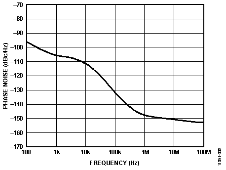
Figure 8. AD9525 ADIsimCLK Simulated Phase Noise Using Bowei MVCO1475 VCO
EVALUATION BOARD SOFTWARE
The AD9525 evaluation software allows the user to control the full functionality of the AD9525 through SPI/I2C communication on the evaluation board. Use the following instructions to set up the AD9525 evaluation board software.
Software Installation
Do not connect the evaluation board until the software installation is complete.
- The latest evaluation software and documentation can be downloaded from http://www.analog.com/en/clock-and-timing/clock-generation-and-distribution/ad9525/products/product.html.
- On the AD9525 Evaluation Board page, double-click AD9525Eval_Setup1.1.0.exe. (Note that the website may have a newer version.) Follow the installation instructions.
Running the Software
Power up and connect the evaluation board to the PC. See the Evaluation Board Hardware section for details on the various connectors on the evaluation board.
- Windows® may automatically detect the evaluation board after the board is first plugged in. Allow Windows® to install the device drivers.

Figure 9. Device Hardware Installation - Double-click AD9525 Evaluation Software to run the AD9525 software. If the evaluation board is found by the software, AD9525 Evaluation Board in green is displayed in the lower left corner of the main window (see Figure 12). If the evaluation board was not found, No Hardware Connected! in red is displayed in the lower left corner of the window.
- If the evaluation board is found, proceed to the Evaluation Software Components section for details about running the software. If the evaluation board is not found, click File > Select Hardware. Select the appropriate AD9525 evaluation board connected and press OK.

Figure 10. Select Hardware Window
AD9525 Evaluation Board in green should be displayed in the bottom left corner of the main window. Alternatively, you can use the software in standalone mode. The standalone mode is useful for verifying register settings for a given PLL setup.See the Evaluation Software Components section for a description of the evaluation software features, and see the Quick Start Guide to the AD9525 PLL section for information about the individual blocks of the AD9525.
QUICK START GUIDE TO THE AD9525 PLL
The AD9525 quick start guide is intended for direct use with the AD9525/PCBZ-VCO evaluation board containing a prepopulated Z-COMM CRO2950B-LF external VCO. Although the AD9525/PCBZ can be populated with a different external VCO/VCXO, the settings discussed in this quick start guide may not be directly applicable. This guide covers only simple PLL operation to lock the PLL. See the AD9525 data sheet and the Evaluation Software Components section for a detailed explanation of the various AD9525 features.
The AD9525 website contains a setup file to configure the AD9525/PCBZ-VCO to the settings discussed in this section. The setup file can be found online here. After being downloaded, the setup file can be loaded into the evaluation board by opening the AD9525 evaluation software, selecting Load Setup from the File menu, and selecting the appropriate .stp file. The values in Table 5 are used for the example discussed in the Quick Start Steps section.
| Parameter | Values |
|---|---|
| Input Frequency | 122.88MHz on REFA |
| Output Frequency | 2949.12 MHz |
| Reference Divider | 2 |
| Phase Detector Frequency | 61.44 MHz |
| Feedback Divider (N divider) | 48 |
| VCO Frequency | 2949.12 MHz |
| VCO Divider (M Divider) | 1 |
| Charge Pump Current (ICP) | 8x |
Table 5. Example Values for Quick Start Steps
Quick Start Steps
When the evaluation software is installed, the evaluation board is connected, and the software is loaded, use the following steps to configure and lock the PLL. These steps assume that the input signal is present to REF A, that the evaluation board has not been modified, and that the PLL loop filter is suitable for a given application.
- Type the intended reference input frequency (in megahertz) in the REF A MHz box at the upper left corner of the main window and press ENTER.
- Type the appropriate RA divider value in the REF INPUTS block and press ENTER. The box surrounding the value of REF A should be outlined in black and illuminated, and the mux symbol should show the REF A signal going to the PFD (see Figure 11). If other references, such as REF B or REF C, are lit, they do not become active until they are selected by the mux.

Figure 11. Reference Inputs Block - Program the N (feedback) divider by clicking the N text box inside of the green APLL block (see Figure 12) Type the desired value and press ENTER. For this example, N = 48 is used (see Figure 12). Note that the N divider is limited to the range of values that can be obtained by multiplying the B and P dividers. See the AD9525 data sheet for more details.
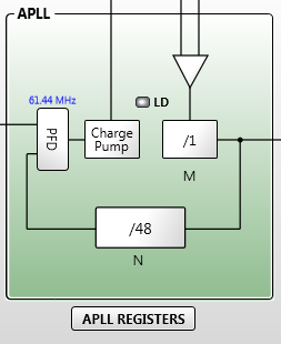
Figure 12. APLL Block - Set the charge pump current multiplier (8× in this case) by clicking APLL Registers, located under the green APLL block, and selecting 8x (default) from the Charge Pump Current drop-down menu (see Figure 19).
- Set the VCO divider (M divider) by clicking the M text box in the green APLL block (see Figure 12). Type the preferred divide value (1 in this case) and press ENTER. Note that both the N divider and M divider make up the NTOTAL divider. The NTOTAL is detailed in the AD9525 data sheet.
- The output frequency of the AD9525 is then displayed in the Output Frequency box on the right side of the window.

Figure 13. Output Frequency Box - Power down any unused drivers by clicking DIST REGISTERS, located under the blue OUTPUT DIST block (see Figure 14) on the right side of the main window. The Distribution window opens.
- Check that each output is powered off in the Power Down PECL Driver box of the Distribution window, and then click Load near the bottom of the window for these settings to be programmed into the evaluation board (see Figure 14).
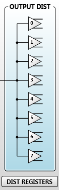
Figure 14. Output Distribution Block - The PLL is then locked. This is indicated in the software by the small square labeled LD in the center of the green APLL block illuminating bright green (see Figure 15).

Figure 15. Software Lock Detect Indicator
resources/eval/ad9525-user-guide.txt · Last modified: 03 Jan 2021 22:11 by Robin Getz