


This version (25 Apr 2022 10:03) was approved by John Xavier Toledo.The Previously approved version (03 Nov 2016 16:17) is available.
Table of Contents
EVALUATING THE AD9250/6673 ANALOG-TO-DIGITAL CONVERTERS
Preface
This user guide describes the AD9250 and AD6673 evaluation boards, AD9250-170EBZ, AD9250-250EBZ and AD6673-250EBZ, which provide all of the support circuitry required to operate these parts in their various modes and configurations. The application software used to interface with the devices is also described.
The AD9250 and AD6673 data sheets provide additional information and should be consulted when using the evaluation board. All documents and software tools are available at www.analog.com/hsadcevalboard. For additional information or questions, send an email to highspeedproductssupport@analog.com.
Typical Measurement Setup

Figure 1. Evaluation Board Connection—AD9250-170EBZ, AD9250-250EBZ or
AD6673-250EBZ(on Left) and HSC-ADC-EVALEZ (on Right)
Features
- SPI interface for setup and control
- Balun/transformer or amplifier input drive option
- FMC Compatible Board, No external supplies required
- VisualAnalog® and SPI controller software interfaces
Helpful Documents
- High Speed ADC Capture Evaluation Kit Rev E (HSC-ADC-EVALEZ)
- AN-905 Application Note, VisualAnalog Converter Evaluation Tool Version 1.0 User Manual
- AN-878 Application Note, High Speed ADC SPI Control Software
- AN-877 Application Note, Interfacing to High Speed ADCs via SPI
- AN-835 Application Note, Understanding ADC Testing and Evaluation
- User Guide for AD6673, User Guide for the AD6673
Software Needed
Design and Integration Files
- Schematic: ad9250_250ebz_sch.pdf
- Layout: ad9250_250ebz_lay.pdf
- Bill of Material: ad9250_250ebz_bom.xls
- MCS File: ad9250_evalez
- SPI Controller Macro File: ad9250_m2i2_spi_mgp.zip
Equipment Needed
- Analog signal source and antialiasing filter
- Sample clock source
- Switching power supply (12.0 V, 3.3 A)
- PC running Windows®
- USB 2.0 port
- AD9250-250EBZ board
- HSC-ADC-EVALEZ FPGA-based data capture kit
Getting Started
This section provides quick start procedures for using the AD9250-170EBZ, AD9250-250EBZ or AD6673-250EBZ board. Both the default and optional settings are described.
Configuring the Board
Before using the software for testing, configure the evaluation board as follows:
- Connect the evaluation board to the data capture board, as shown in Figure 1.
- Connect one 12V, 3.3A switching power supply (such as the V-Infinity ETSA120330UDC-P5P-SZ supplied) to the HSC-ADC-EVALEZ board. Note: Make sure the 12V power supply is used.
- Connect the HSC-ADC-EVALEZ board to the PC with a USB cable. (Connect to P702.)
- On the AD9250 EVB, provide a clean, low jitter clock source to the connector labeled CLKIN at the desired ADC conversion rate with power level set between 10dBm and 14dBm.
- On the ADC evaluation board, use a clean signal generator with low phase noise to provide an input signal to the analog input at connector J100 (Channel A) and/or J200 (Channel B). Use a 1 m, shielded, RG 58, 50 Ω coaxial cable to connect the signal generator. For best results use a narrow-band, band-pass filter with 50 Ω terminations and an appropriate center frequency. (ADI uses TTE, Allen Avionics, and K and L band-pass filters.) In order for the input level to be near the ADC’s full scale, the generator level should be set to 8dBm to 12dBm – this level depends on the input frequency and any losses in bandpass filters.
Setting up the ADC Data Capture
After configuring the board, set up the ADC data capture using the following steps:
- Open VisualAnalog on the connected PC. The appropriate part type should be listed in the status bar of the VisualAnalog – New Canvas window. Select the template that corresponds to the type of testing to be performed (see Figure 2, where the AD9250 or AD6673 is shown as example).

Figure 2. VisualAnalog, New Canvas Window
- After the template is selected, a message appears asking if the default configuration can be used to program the FPGA (Figure 3). Click YES and the window closes.

Figure 3. VisualAnalog Default Configuration Message
- To change features to settings other than the default settings, click the Expand Display button, located on the bottom right corner of the window, to see what is shown in Figure 5. Detailed instructions for changing the features and capture settings can be found in the AN-905 Application Note, VisualAnalog Converter Evaluation Tool Version 1.0 User Manual. After the changes are made to the capture settings, click the Collapse Display button (see Figure 4).


Figure 4. VisualAnalog Window Toolbar, Collapsed Display

Figure 5. VisualAnalog, Main Window Expanded Display
Evaluation and Test
Setting up the SPI Controller Software
After the ADC data capture board setup is complete, set up the SPI controller software using the following procedure:
- Open the SPI controller software by going to the Start menu or by double-clicking the SPIController software desktop icon. If prompted for a configuration file, select the appropriate one. If not, check the title bar of the window to determine which configuration is loaded. If necessary, choose Cfg Open from the File menu and select the appropriate file based on your part type. Note that the CHIP ID(1) box should be filled to indicate whether the correct SPI controller configuration file is loaded (see Figure 6).

Figure 6. SPI Controller, CHIP ID(1) Box
- Click the New DUT button in the SPIController window (see Figure 7).

Figure 7. SPI Controller, New DUT Button
- In the ADCBase 0 tab of the SPIController window, find the CLOCK DIVIDE(B) box (see Figure 8). If using the clock divider, use the drop-down box to select the correct clock divide ratio, if necessary. See the appropriate part data sheet, the AN-878 Application Note, High Speed ADC SPI Control Software, and the AN-877 Application Note, Interfacing to High Speed ADCs via SPI, for additional information on the available settings.

Figure 8. SPI Controller, ADCBase0 Page
- Note that other settings can be changed on the ADCBase 0 page (see Figure 8) and the ADC A and ADC B pages (see Figure 9) to set up the part in the desired mode. The ADCBase 0 page settings affect the entire part, whereas the settings on the ADC A and ADC B pages affect the selected channel only. See the appropriate part data sheet; the AN-878 Application Note, High Speed ADC SPI Control Software, and the AN-877 Application Note, Interfacing to High Speed ADCs via SPI, for additional information on the available settings.
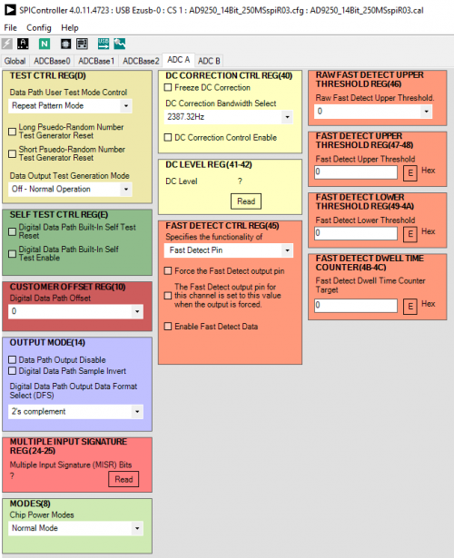
Figure 9. SPI Controller, Example ADC A Page
- Click the Run button in the VisualAnalog toolbar (see Figure 10).

Figure 10. Run Button (Encircled in Red) in VisualAnalog Toolbar, Collapsed Display


Adjusting the Amplitude of the Input Signal
The next step is to adjust the amplitude of the input signal for each channel as follows:
- Adjust the amplitude of the input signal so that the fundamental is at -1.0 dBFS. Examine the Fund Power reading in the left panel of the VisualAnalog Graph - AD9250 Average FFT window (see Figure 11) to verify this.

Figure 11. Graph Window of VisualAnalog
- Repeat this procedure for Channel B.
- Click the disk icon within the Graph window to save the performance plot data as .csv formatted file. See Figure 12 for AD9250 example. Please refer to the respective data sheet of the product of interest for its typical FFT performance.

Figure 12. Typical FFT, AD9250


Optional Steps
The following steps below are optional steps for validation of SPI Control:
- Force the data output of ADC A and/or ADC B to generate a long PN sequence as shown in Figure 13.

Figure 13. SPI Control for PN Long Sequence Validation
- Results in the noise floor of the selected ADC's FFT to increase significantly as shown in Figure 14.

Figure 14. Increased Noise Floor on FFT
- To re-program the FPGA, select the ADC Data Capture Settings window and click on the ‘Capture Board’ tab (see the box in the figure below). In the FPGA box select the program “ad9250_evalez.mcs” to configure the FPGA. After selecting the file, click the “Program” button to download the file to the FPGA. The ‘CONFIG_DONE’ LED should illuminate on the HSC-ADC-EVALEZ board indicating that the FPGA is now programmed.


Troubleshooting Tips
If the FFT plot appears abnormal, do the following:
- If you see a normal noise floor when you disconnect the signal generator from the analog input, be sure you are not overdriving the ADC. Reduce the input level, if necessary.
- In VisualAnalog, click the Settings button in the Input Formatter block. Check that Number Format is set to correct encoding (2's complement by default).
If the FFT appears normal but the performance is poor, check the following:
- Make sure that an appropriate filter is used on the analog input.
- Make sure that the signal generators for the clock and the analog input are clean (low phase noise).
- Change the analog input frequency slightly if noncoherent sampling is being used.
- Make sure that the SPI configuration file matches the product being evaluated.
If the FFT window remains blank after Run is clicked, do the following:
- Make sure that the evaluation board is securely connected to the HSC-ADC-EVALEZ board.
- Disconnect power from both the ADC evaluation board and the HSC-ADC-EVALEZ board, disconnect the USB cable from the HSC-ADC-EVALEZ board and begin again at Step 1.
- Make sure that the FPGA has been programmed by verifying that the CONFIG_DONE LED is illuminated on the HSC-ADC-EVALEZ board.
- Make sure that the correct FPGA program was installed.
If VisualAnalog indicates that the FIFO Capture timed out, do the following:
- Make sure that all power and USB connections are secure.
- Double check that the encode clock source is present at the CLKIN connector.
resources/eval/ad9250-ad6673ebz.txt · Last modified: 25 Apr 2022 10:03 by John Xavier Toledo